Nano capacitor and electronic ballast using same

A capacitor and micro-capacitor technology, applied in capacitors, fixed capacitors, multiple fixed capacitors, etc., can solve the problems of poor working stability and reliability, poor high temperature resistance, and poor temperature resistance, so as to improve working reliability and performance. Stability, lower temperature rise, small size effect

Inactive Publication Date: 2010-03-10
WEINA LIGHTING ENERGY SAVING NANO TECH CHENGDU
View PDF4 Cites 0 Cited by
  • Summary
  • Abstract
  • Description
  • Claims
  • Application Information

AI Technical Summary

Problems solved by technology

[0004] The purpose of the present invention is to overcome the above-mentioned shortcomings of poor high temperature resistance, poor working stability and reliability existing in capacitors in existing electronic ballasts, and provide users with a parallel connection of micro capacitors with a large number of nanoscale structure sizes. Composition, better heat dissipation, high temperature resistance, smaller size, improved current operating characteristics, and nano capacitors with longer working life, thus effectively solving the long-standing problem of electronic ballasts due to poor temperature resistance of capacitors. , Poor reliability, prone to the problem of capacitor explosion

Method used


Image

  • Nano capacitor and electronic ballast using same
  • Nano capacitor and electronic ballast using same

Examples


Embodiment 1

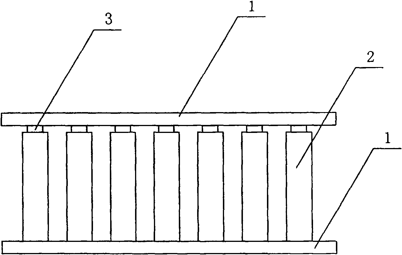
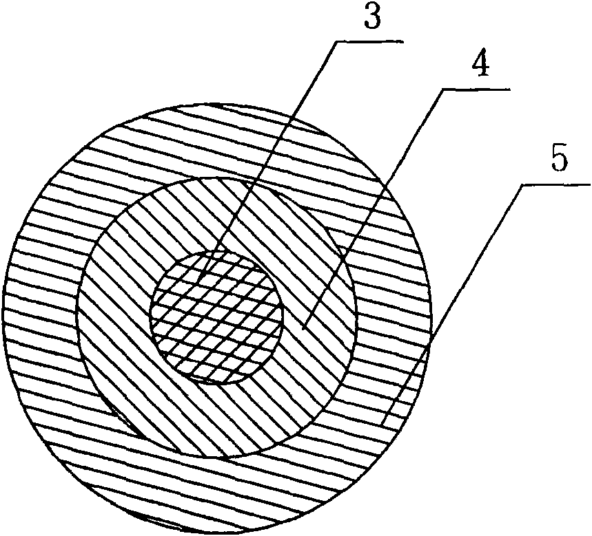
[0027] Embodiment 1: as figure 2 As shown, the inner layer conductor 3 of the microcapacitor 2 of the nanocapacitor in the present embodiment is a multi-walled carbon nanotube with an average diameter of 80 nanometers, and a height of 10 microns. The inner layer conductor 3 is on the base of the metal aluminum electrode grown vertically. Then, the outer surface of the inner layer conductor 3 is coated with a layer of aluminum oxide annular film insulator as the interlayer insulator 4 (medium), and its thickness is 10 microns, and then the outer surface of the interlayer insulator 4 is coated with a layer of insulator. The gap between the insulator and the interlayer insulator 4 is filled with aluminum as the outer layer conductor 5, and its thickness is less than 100 nanometers. Such as figure 1 As shown, the electrode 1 of the nanocapacitor is a flat film electrode, and there are many microcapacitors 2 connected in parallel between the electrodes 1, the number of which is ...

Embodiment 2

[0030] Embodiment 2: as figure 2 As shown, the inner layer conductor 3 of the microcapacitor 2 in the present embodiment is an aluminum wire structure with an average diameter of 90 nanometers and a height of 20 microns, which is called an aluminum nanowire. The inner layer conductor 3 is on the base of the metal aluminum electrode It is grown vertically, and then oxidized a layer of ring-shaped thin-film insulating aluminum oxide on the inner layer conductor 3 as the interlayer insulator 4 (dielectric), with a thickness of 10 microns, and then coating a layer on the interlayer insulator 4 (dielectric). Aluminum with a layer thickness of 10 μm serves as the outer conductor 5 . Such as figure 1 As shown, the electrode 1 of the nanocapacitor is a flat film electrode, and there are many microcapacitors 2 connected in parallel between the electrodes 1, the number of which is determined according to the capacity. The layer conductor 3 is connected to the upper electrode 1 , and ...

Embodiment 3

[0033] Embodiment 3: as figure 2 As shown, the inner layer conductor 3 of the microcapacitor 2 of the nanocapacitor in the present embodiment is a multi-walled carbon nanotube with an average diameter of 80 nanometers, and a height of 10 microns. The inner layer conductor 3 is on the base of the metal aluminum electrode grown vertically. Then, the outer surface of the inner layer conductor 3 is coated with a layer of aluminum oxide annular film insulator as the interlayer insulator 4 (medium), and its thickness is 90 nanometers, and then the outer surface of the interlayer insulator 4 is coated with a layer of insulator. The gap between the insulator and the interlayer insulator 4 is filled with aluminum as the outer layer conductor 5 with a thickness of 10 microns. Such as figure 1 As shown, the electrode 1 of the nanocapacitor is a flat film electrode, and there are many microcapacitors 2 in parallel between the electrodes 1, the number of which is determined according to...


PUM


Abstract

The Nano capacitor is composed of multiple microcapacitors with structure size in Nano level formed between two tabulate membrane electrodes. The microcapacitor is in columniform laminar structure: inner and outer layers are conductors connected to tabulate membrane electrodes respectively; intermediate layer is an insulative medium; diameter of inner conductor is less than 100 Nano; and thicknessof intermediate medium and outer conductor is between tens of Nano and 100 micros. Comparing with current products, the disclosed Nano capacitor possesses advantages of good resistance to high temperature, doubled service life, and reduced size more than 100 times. The disclosed Nano capacitor is applicable to electronic products with high requirement and under high working temperature such as electronic ballast of discharge lamp in high intensity.

Description

technical field [0001] The present invention relates to a component in the field of nanoelectronics technology and a lighting lamp fitting using the component, specifically, a nanocapacitor used in an electronic ballast for a high-intensity glow discharge lamp and the nanocapacitor using the nanocapacitor electronic ballasts. Background technique [0002] The existing electronic ballast designs are all based on traditional electronic materials and components. Their materials are characterized by amorphous or polycrystalline forms, and the size of the disordered or ordered particles is at least greater than 0.1 micron. The device is mainly used for low-power electronic products or electronic ballasts for low-intensity lighting lamps. When it is used for high-power or high-intensity discharge lighting lamps, it usually requires higher trigger voltage and frequency to meet the requirements of normal use. Problems such as large power consumption and temperature rise of the conv...

Claims


Application Information

Patent Timeline
Patent Type & Authority Patents(China)
IPC IPC(8): H01G4/38H01G4/00B82B1/00H05B41/14
Inventor 韩杰杨毅陈德甫
Owner WEINA LIGHTING ENERGY SAVING NANO TECH CHENGDU
Why Eureka
Try Eureka