Semiconductor structure

A semiconductor and connection structure technology, applied in the direction of transistors, etc., can solve the problems of the performance of radio frequency switching devices that need to be improved, and achieve the effect of reducing the equivalent resistance value and improving performance

Inactive Publication Date: 2018-02-27
SHANGHAI HUAHONG GRACE SEMICON MFG CORP
View PDF6 Cites 0 Cited by
  • Summary
  • Abstract
  • Description
  • Claims
  • Application Information

AI Technical Summary

Problems solved by technology

[0004] However, the performance of the RF switching devices formed in the prior art needs to be improved

Method used


Image

  • Semiconductor structure
  • Semiconductor structure

Examples


Embodiment Construction

[0019] In order to make the objects, features and advantages of the present invention more comprehensible, please refer to the accompanying drawings. It should be noted that the structures, proportions, sizes, etc. shown in the drawings attached to this specification are only used to match the content disclosed in the specification, for those who are familiar with this technology to understand and read, and are not used to limit the implementation of the present invention. Limiting conditions, so it has no technical substantive meaning, any modification of structure, change of proportional relationship or adjustment of size, without affecting the effect and purpose of the present invention, should still fall within the scope of the present invention. The disclosed technical content must be within the scope covered.

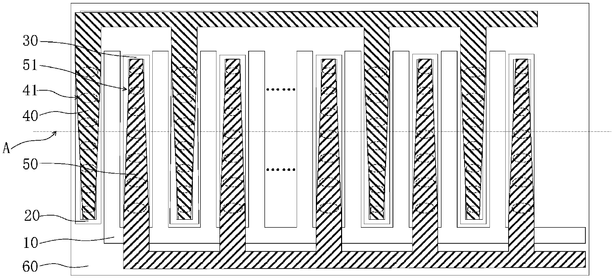
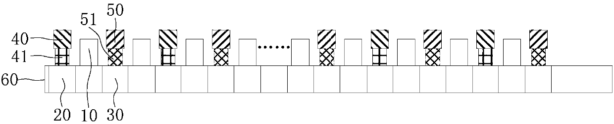
[0020] Such as figure 1 with figure 2 As shown, the present invention provides a semiconductor structure, which includes a gate 10, a first doped region 20, a ...


PUM


Abstract

The invention provides a semiconductor structure. The semiconductor structure comprises grid electrodes, first doped areas, second doped areas, first connection structures and second connection structures, wherein the strip-type grid electrodes are located on the a substrate, the first doped areas and the second doped areas are located on the two sides of the grid electrodes respectively and extend to the stretching direction of the grid electrodes, the first connection structures are connected with the first doped areas, and the second connection structures are connected with the second dopedareas. The cross sections of the first connection structures are progressively increased in the extending direction of the grid electrodes, and the cross sections of the second connection structuresare progressively increased in the extending direction of the grid electrodes and in the direction opposite to the progressive increase direction of the first connection structures. In the semiconductor structure, the cross sections of the first connection structures are progressively increased in the extending direction of the grid electrodes, and meanwhile, the cross sections of the second connection structures are progressively increased in the extending direction of the grid electrodes and in the direction opposite to the progressive increase direction of the first connection structures, so that the performance of the semiconductor structure is improved.

Description

technical field [0001] The invention relates to the technical field of semiconductors, in particular to a semiconductor structure. Background technique [0002] In the field of semiconductor technology, with the continuous development of technology, the requirements for semiconductor devices are also getting higher and higher. Among them, the radio frequency switching device is an important switching device as a signal switch in the communication field, and can be applied to wired transmission of radio frequency signals. [0003] When the radio frequency switching device is working, some areas are in a conduction state, and some areas are in an off state. The performance of the radio frequency switching device or the characteristic test parameters of the process can be evaluated by a Figure of Merit (FOM). FOM=Ron*Coff, where Ron is the equivalent resistance value when the RF switching device is in the on state, Coff is the equivalent capacitance value when the RF switchin...

Claims


Application Information

Patent Timeline
Patent Type & Authority Applications(China)
IPC IPC(8): H01L27/088
CPCH01L27/088
Inventor 刘张李
Owner SHANGHAI HUAHONG GRACE SEMICON MFG CORP
Why Eureka
Try Eureka