
Transfer printing method, photomask for transfer printing and manufacturing method thereof

A photomask and graphics technology, applied in the field of transfer photomask and its manufacturing, can solve the problems of key scale differences, and achieve the effect of narrowing the gap and reducing errors

Inactive Publication Date: 2010-07-21
SEMICON MFG INT (SHANGHAI) CORP
View PDF0 Cites 1 Cited by
  • Summary
  • Abstract
  • Description
  • Claims
  • Application Information

AI Technical Summary

Problems solved by technology

[0005] In the photomask of the prior art, the graphic load of the graphic area and the graphic load of the border area are very different, and there will be subtle differences in the key dimensions of the edge part and the central part of the photomask graphic area

Method used


Image

  • Transfer printing method, photomask for transfer printing and manufacturing method thereof
  • Transfer printing method, photomask for transfer printing and manufacturing method thereof
  • Transfer printing method, photomask for transfer printing and manufacturing method thereof

Examples


Embodiment Construction

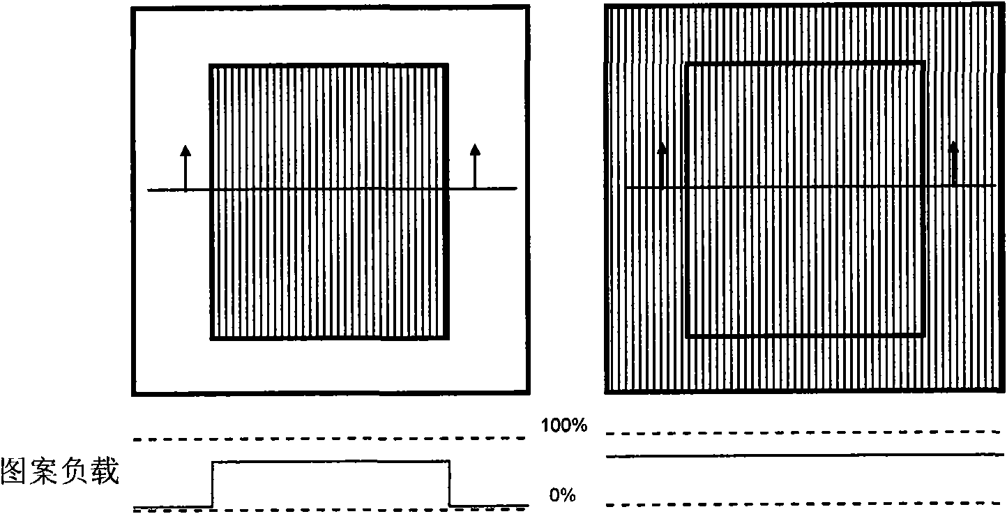
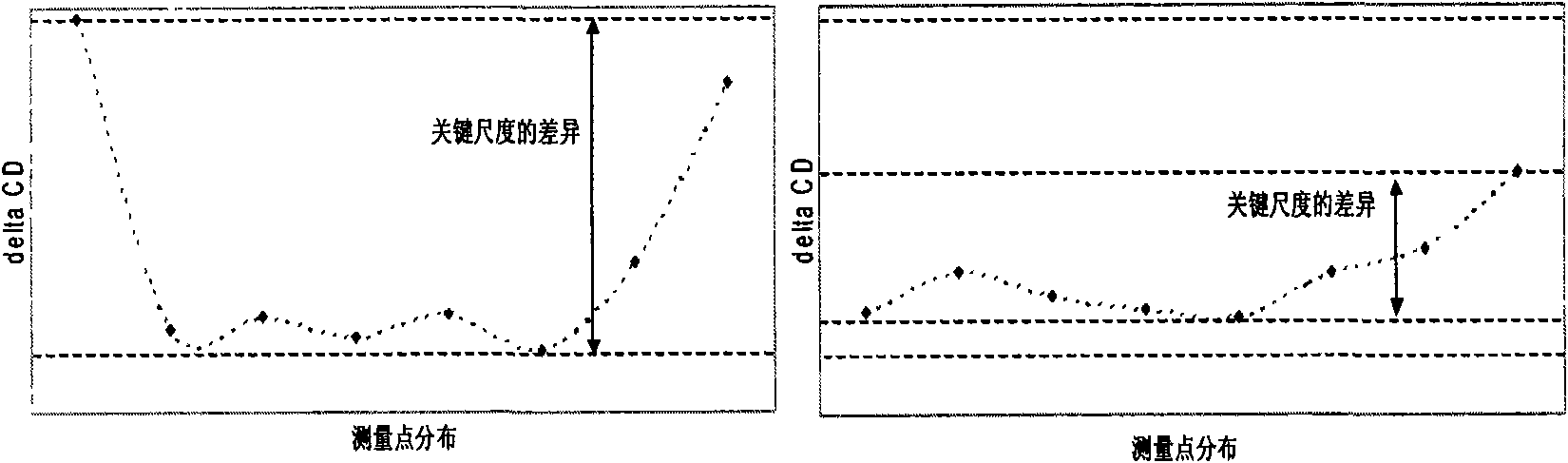
[0027] Figure 4 A schematic diagram of the principle of the solution of the present invention is shown. 401 is the main graphic to be transferred to the wafer, with a certain graphic load; 402 is a graphic corresponding to the preset frame graphic data, and the graphic has a graphic load close to that of the graphic 401 . The scheme of the present invention combines 401 and 402 to generate a photomask 403. The main pattern area of ​​the photomask 403 has a figure as shown in 401, and the border area has a figure as shown in 402, so that the figure on the edge of the pattern area The load will not change drastically.

[0028] In order to make the object, technical solution and advantages of the present invention clearer, the present invention will be further elaborated below in conjunction with specific examples.

[0029] Embodiment 1 of the present invention proposes a method for manufacturing a photomask. Various types of frame pattern data are prepared in advance. The fra...


PUM


Abstract

The invention discloses a method of manufacturing a photomask. In the method, a plurality of types of optional border graphic data corresponding to border areas of a photomask are needed to be prepared in advance, and border graphic data of each type is provided with a preset graphic load. The method comprises the following steps: obtaining a graphic load of graphic data corresponding to the main graphic area of a photomask; selecting optional border graphic data with the graphic load closest to the obtained main graphic load; combining the border graphic data with the main graphic data to generate an exposure file; and exposing the exposure file on a blank substrate for the photomask, developing photoresist of the substrate, etching the shading layer of the substrate and removing the photoresist, thereby obtaining the photoresist. The invention also discloses a photomask and a transfer printing method. Moreover, the invention can reduce the influence of the graphic load difference of the border area and the main graphic area of the photomask on the key scale of the photomask.

Description

technical field [0001] The invention relates to the technical field of integrated circuit manufacturing, in particular to a transfer printing method, a photomask used for transfer printing and a manufacturing method thereof. Background technique [0002] In the integrated circuit manufacturing process, it is necessary to define extremely fine-sized patterns on the wafer. These patterns are formed by first placing a photomask on the wafer coated with photoresist. When the wafer is exposed, the photoresist material of the wafer under the light-transmitting part of the photomask pattern undergoes a chemical reaction, thereby faithfully transferring the pattern of the photomask onto the wafer. [0003] figure 1 A cross-sectional view of a photomask blank substrate is shown. The photomask that has not been subjected to microdevelopment processing is called a photomask blank substrate. The blank substrate includes three sublayers, which are photoresist 101 , mask light-shieldin...

Claims


Application Information

Patent Timeline
IPC IPC(8): G03F1/14G03F7/00G03F1/68
Inventor 田明静
Owner SEMICON MFG INT (SHANGHAI) CORP
Learn More