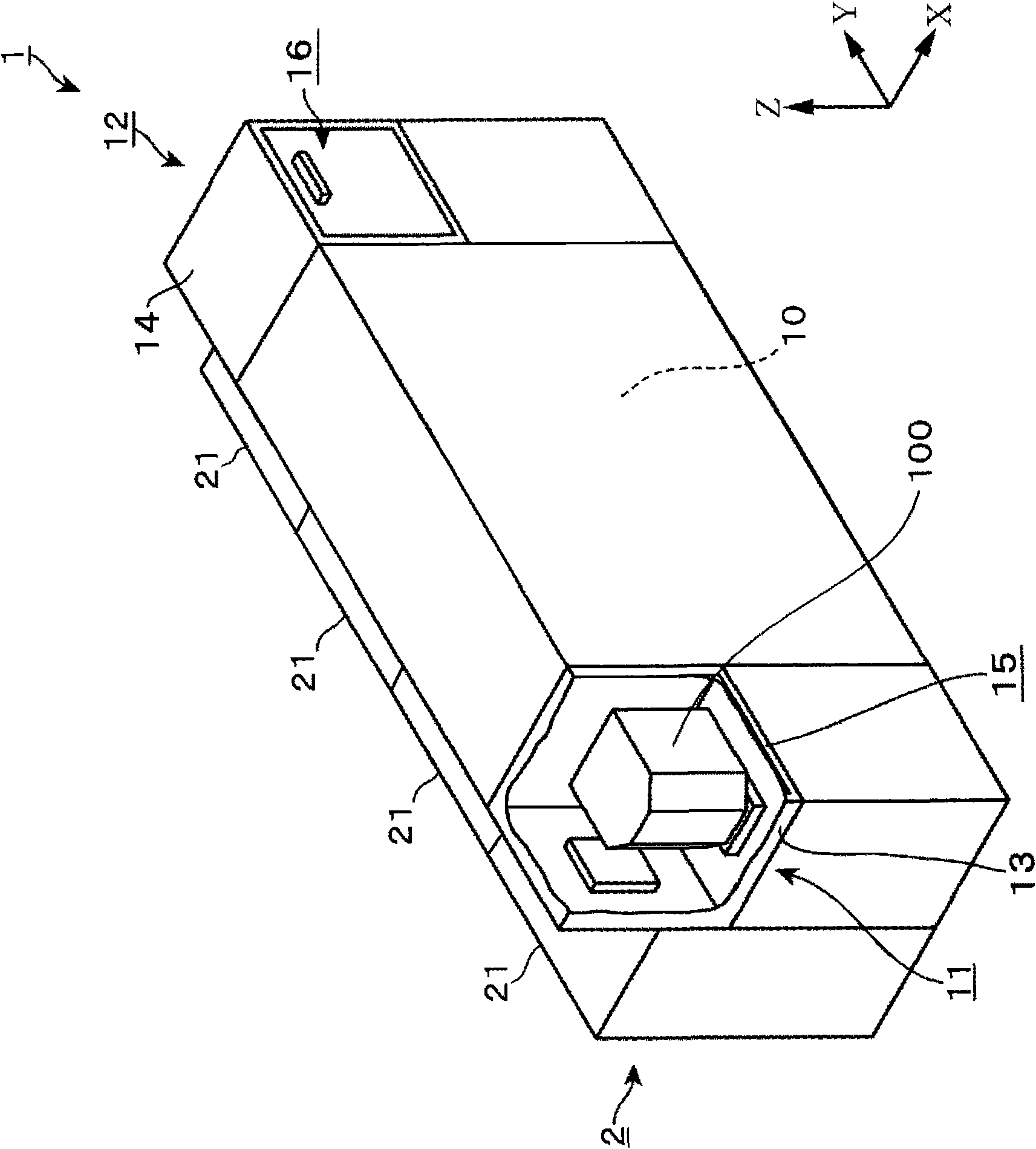
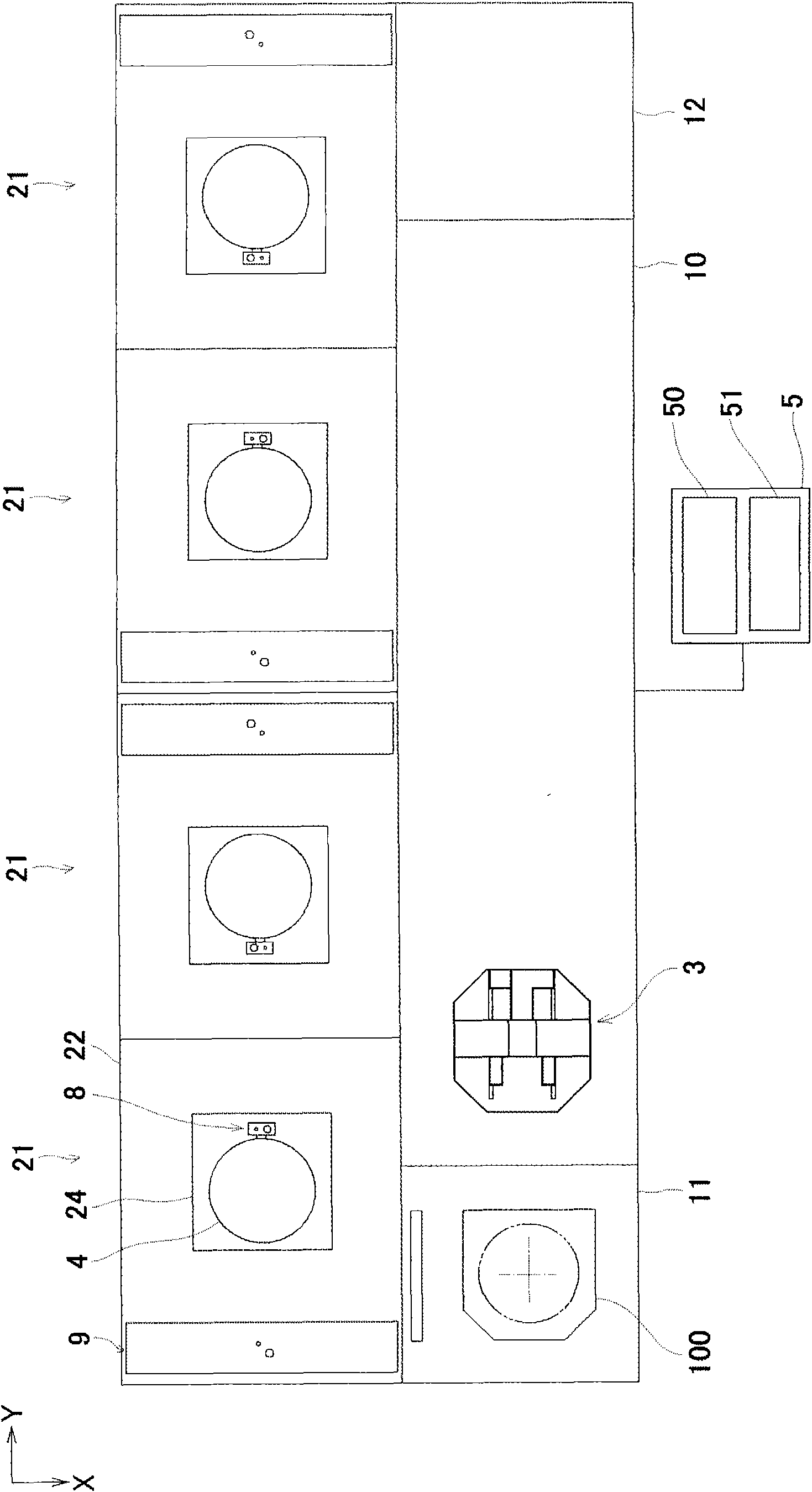
Probe device

A technology of detectors and mounting tables, which is applied in the direction of measuring devices, instruments, and parts of electrical measuring instruments, etc., which can solve unsatisfactory large-scale devices, longer standby time of inspection parts, and lower detector test processing capabilities, etc. problem, achieve the effect of shortening the standby time and suppressing the reduction of processing capacity

Active Publication Date: 2010-07-21
TOKYO ELECTRON LTD
View PDF1 Cites 14 Cited by
  • Summary
  • Abstract
  • Description
  • Claims
  • Application Information

AI Technical Summary

Problems solved by technology

Therefore, there is a problem that the standby time of the inspection unit becomes longer corresponding to the time for performing the pre-alignment, and the throughput of the detector test decreases.
Since the miniaturization of the detector device has been required in recent years, the upsizing of the device is unsatisfactory

Method used


Image

  • Probe device
  • Probe device
  • Probe device

Examples


no. 2 Embodiment approach

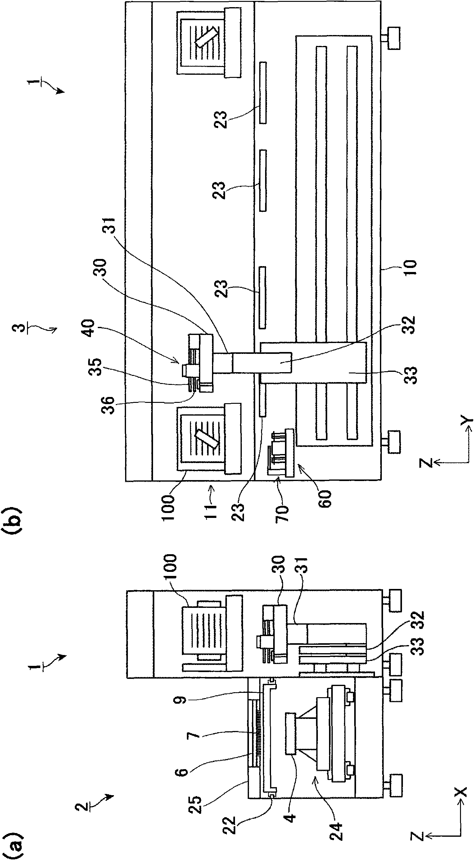
[0080] refer to Figure 13 to Figure 16 A detector device according to a second embodiment of the present invention will be described. The probe device of the second embodiment is the same as that of the first embodiment except for the structure of the substrate holding device 170 , and therefore, the same or equivalent parts as those of the first embodiment will be described with the same reference numerals. In the first embodiment, the substrate holding device 70 only suction-holds the wafer W. However, in the substrate holding device 170 of the present embodiment, pre-alignment of the held wafer W can be performed as necessary.

[0081] In this embodiment, if Figure 13 , Figure 14 As shown, an installation portion 168 is provided on the upper surface of the base 61 of the substrate storage portion 60 . The setting portion 168 has a flat plate 169 forming a horizontal plane in an area above the substrate storage portion 60 , and the substrate holding device 170 is provi...


PUM


Abstract

The invention provides a probe device which can restrain the reduction of processing ability when the maintenance substrate is used to perform maintenance operation of the examination part. The probe device includes a wafer conveying arm with an arm body; a pre-aligning mechanism for perform position aligning to the facing and center of the taken out wafer; a substrate retaining device having an adsorption part for receiving wafer from the wafer conveying arm and performing adsorption holding. When the interrupt processing of the examination part is emitted, the wafer supported on the arm body is held on the substrate retaining device, the arm body is used to take out needle lapping wafer from the substrate containing part and exchange with the wafer of the wafer chuck. Therefore, the standby time of the examination part during needle lapping processing is shortened, and the test processing ability is improved.

Description

technical field [0001] The present invention relates to a probe device for electrically measuring an inspected chip by bringing a probe of a probe card into contact with an electrode pad of an inspected portion of a substrate such as a semiconductor wafer (hereinafter referred to as a wafer). Background technique [0002] Conventionally, a probe test in which a probe such as a probe of a probe card is brought into contact with an electrode pad of an IC chip by using a probe device to investigate electrical characteristics is performed. The probe device includes: a load port; an inspection unit having a probe card and a mounting table; and a transfer chamber provided with a wafer transfer mechanism for transferring a wafer between the load port and the inspection unit. Moreover, the wafer transfer mechanism takes out the wafer from the wafer carrier as the transfer container carried into the loading unit, and performs pre-alignment using the pre-alignment mechanism in the tra...

Claims


Application Information

Patent Timeline
Patent Type & Authority Applications(China)
IPC IPC(8): H01L21/66H01L21/68H01L21/677
CPCB24B19/16G01R1/06711G01R1/07307G01R31/2601
Inventor 带金正
Owner TOKYO ELECTRON LTD
Why Eureka
Try Eureka