Diode ceramic packaging template
A technology of ceramic packaging and ceramic plates, which is applied in the direction of electrical components, electric solid devices, circuits, etc., can solve the problems of short service life, non-wearable plastic templates, and decreased yield, and achieve the effect of long service life
- Summary
- Abstract
- Description
- Claims
- Application Information
AI Technical Summary
Problems solved by technology
Method used
Image
Examples
Embodiment Construction
[0021] The present invention will be described in detail below in conjunction with the accompanying drawings.
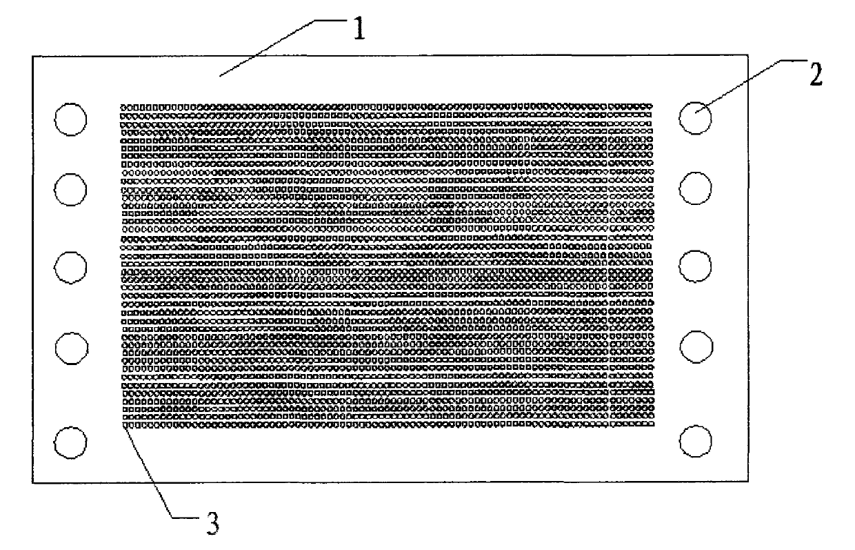
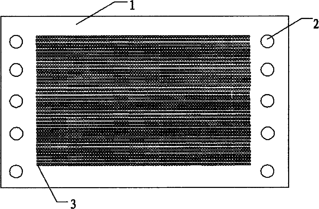
[0022] A diode ceramic packaging template includes a ceramic board body 1, screw holes 2 are opened on both sides of the ceramic board body 1, and pin positioning round holes 3 are opened in the middle of the ceramic board body 1.
[0023] Preferably, 800 pin positioning circular holes 3 are opened in the middle of the ceramic plate body 1 .
[0024] Preferably, 1000 pin positioning round holes 3 are opened in the middle of the ceramic plate body 1 .
[0025] Preferably, 1280 pin positioning circular holes 3 are opened in the middle of the ceramic plate body 1 .
[0026] Preferably, 1495 pin positioning round holes 3 are opened in the middle of the ceramic plate body 1 .
[0027] Preferably, 1500 pin positioning round holes 3 are opened on the ceramic plate body 1 .
[0028] Preferably, 2280 pin positioning round holes 3 are opened on the ceramic plate body 1 .
...
PUM
 Abstract
Description
Claims
Application Information

