Arrangement comprising at least one semiconductor component, in particular a power semiconductor component for the power control of high currents

A power control and semiconductor technology, which is applied in the field of devices having at least one semiconductor device, especially a power semiconductor device for power control of large currents, can solve the problems of unfavorable mobile applications, expensive devices, large volume, etc., and achieves compactness. structure, avoid temperature hot spots, avoid the effect of overheating problems

Active Publication Date: 2010-08-18
SIEMENS AG
View PDF1 Cites 10 Cited by
  • Summary
  • Abstract
  • Description
  • Claims
  • Application Information

AI Technical Summary

Problems solved by technology

However, such devices are expensive, bulky and correspondingly heavy due to the safety loading required in the electric

Method used


Image

  • Arrangement comprising at least one semiconductor component, in particular a power semiconductor component for the power control of high currents
  • Arrangement comprising at least one semiconductor component, in particular a power semiconductor component for the power control of high currents
  • Arrangement comprising at least one semiconductor component, in particular a power semiconductor component for the power control of high currents

Examples


Embodiment Construction

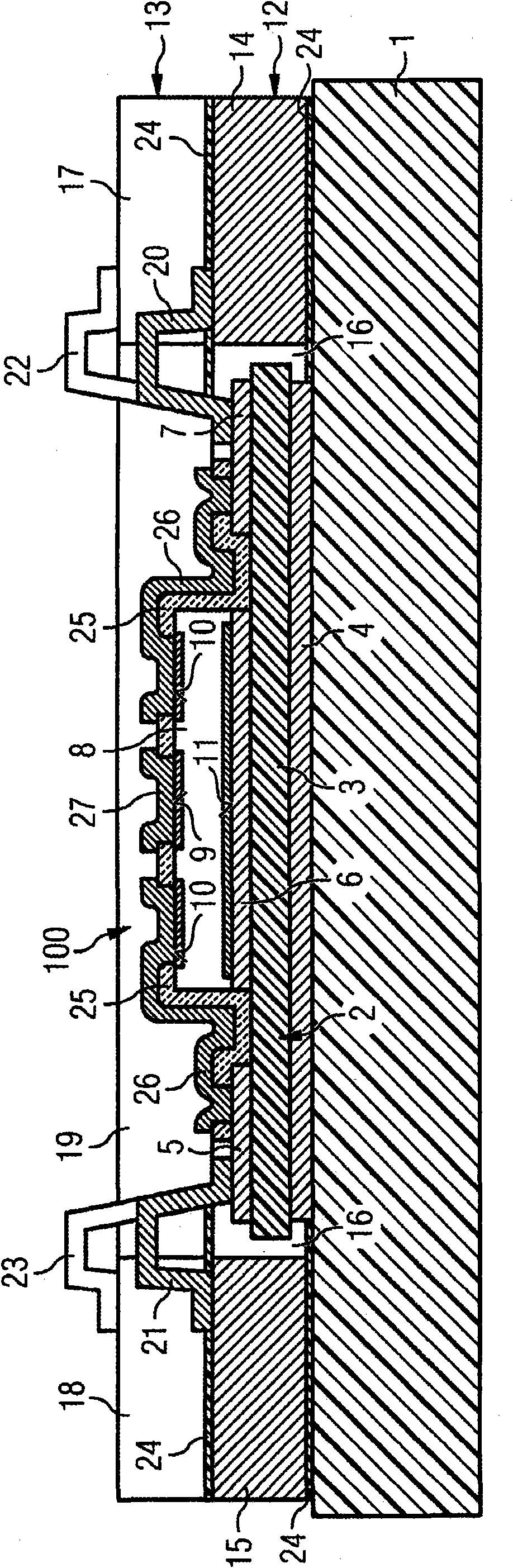
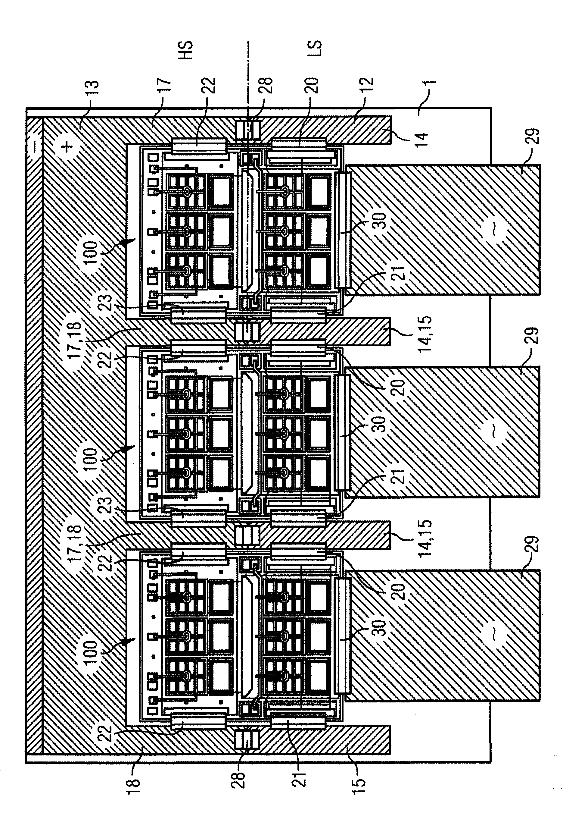
[0034] figure 1 A cross-sectional view of a device according to the invention is shown. The carrier device 2 is applied to the carrier body 1 made of a material that conducts heat well. The carrier device 2 can be designed, for example, as a DCB substrate. DCB stands for direct copper. Alternatively, the use of an AMB substrate (AMB=active metal brazing) is also conceivable. The carrier device 2 comprises a carrier body 3 , which consists of an insulating material (for example ceramics), on the front and rear sides of which carrier body 3 the contact surfaces 4 , 5 , 6 , 7 are formed. The contact surfaces 4 , 5 , 6 , 7 can be applied to the carrier 3 galvanically or by lamination and structuring. The carrier body 3 is connected to the carrier body 1 via a preferably full-surface contact surface 4 arranged on its rear side. This can be done, for example, using solder or other adhesives. Adhesives that conduct heat well are preferably used.

[0035] The contact surfaces 5...


PUM


Abstract

The description is given of an arrangement comprising at least one semiconductor component (8; 101-1, 101-2, 101-3), in particular a power semiconductor component for the power control of high currents, in which the at least one semiconductor component (8; 101-1, 101-2, 101-3) has in each case at least two electrical connection pads arranged separately from one another and is arranged on a commoncarrier body (1) in a manner electrically insulated from the latter. Furthermore a first and a second busbar (12, 13) are fixed on the carrier body (1) alongside the at least one semiconductor component (8; 101-1, 101-2, 101-3) and in a manner electrically insulated from the at least one semiconductor component (8; 101-1, 101-2, 101-3). One electrical connection pad of the at least one semiconductor component (8; 101-1, 101-2, 101-3) is electrically connected to the first busbar (12, 13) and another electrical connection pad of said semiconductor component (8; 101-1, 101-2, 101-3) is electrically connected to the second busbar (12, 13). The first and/or the second busbar (12, 13) have/has sections arranged at opposite sides of the semiconductor component (8; 101-1, 101-2, 101-3), wherein a current is applied to the connection pad electrically connected to the relevant busbar (12, 13) from both sections.

Description

technical field [0001] The invention relates to a device for power control of high currents having at least one semiconductor component, in particular a power semiconductor component. In this arrangement, at least one semiconductor component in each case has at least two electrical connection areas arranged separately from one another and is arranged on the common carrier body in an electrically insulated manner therefrom. The first and the second busbar are attached to the carrier body next to the at least one semiconductor component and electrically insulated from the at least one semiconductor component. An electrical connection area of ​​at least one semiconductor component is electrically connected to the first busbar. A further electrical connection area of ​​the semiconductor component is electrically connected to the second busbar. Background technique [0002] Such a device is described in WO 03 032390 A1. Devices of the described type are used, for example, for ...

Claims


Application Information

Patent Timeline
IPC IPC(8): H01L25/07
CPCH01L2224/24226H01L2224/24051H01L2924/01082H01L2924/13091H01L24/82H01L2924/01019H01L2924/01029H01L2924/19041H01L2924/01013H01L2924/014H01L2924/30107H01L2224/32225H01L2924/01079H01L24/24H01L2924/01068H01L2924/01005H01L2924/01033H01L2924/01006H01L25/072H01L2924/0102H01L2924/01074H01L2924/01078H01L2924/01057H01L2924/01052H01L2924/01075H01L2924/13055H01L2924/1301H01L2224/0603H01L2224/06181H01L2924/00
Inventor G·希梅塔N·塞利格
Owner SIEMENS AG
Why Eureka
Try Eureka