Flexible printed circuit board of flat panel display device

A flexible printed circuit and flat display technology, applied to printed circuit parts, static indicators, etc., can solve the problems of cracking and breaking of leads, and achieve the effect of solving the cracking or breaking of leads under force

Active Publication Date: 2010-09-01
BOE TECH GRP CO LTD +1
View PDF0 Cites 7 Cited by
  • Summary
  • Abstract
  • Description
  • Claims
  • Application Information

AI Technical Summary

Problems solved by technology

[0007] Since the flexible printed circuit board uses a flexible substrate, and the flexible printed circuit board needs to be bent, pulled or twisted during assembly and transportation, it will cause cracking or breaking of the leads made of copper foil in the exposed area

Method used


Image

  • Flexible printed circuit board of flat panel display device
  • Flexible printed circuit board of flat panel display device
  • Flexible printed circuit board of flat panel display device

Examples


Embodiment Construction

[0018] The technical solutions of the present invention will be described in further detail below with reference to the accompanying drawings and embodiments.

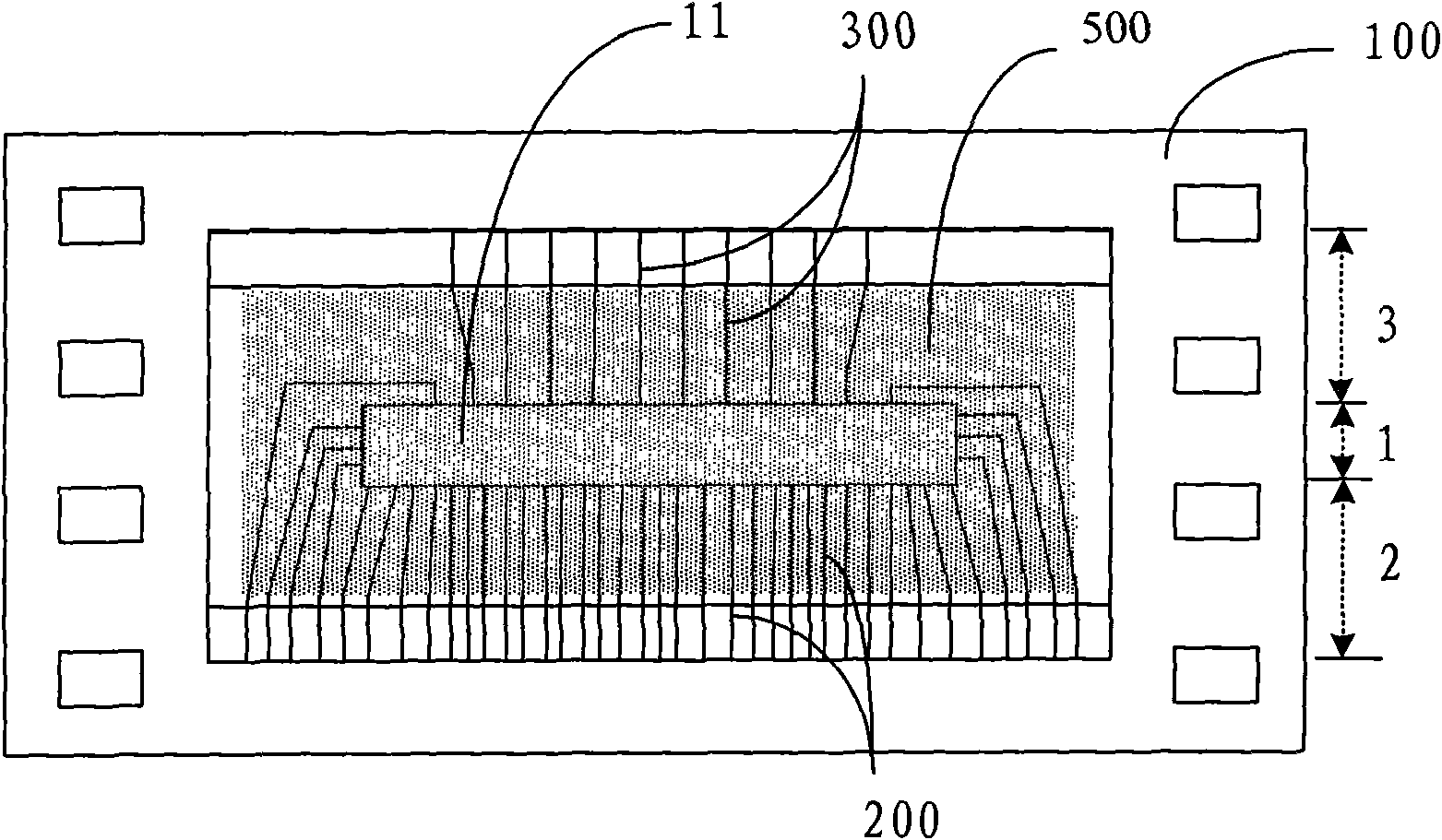
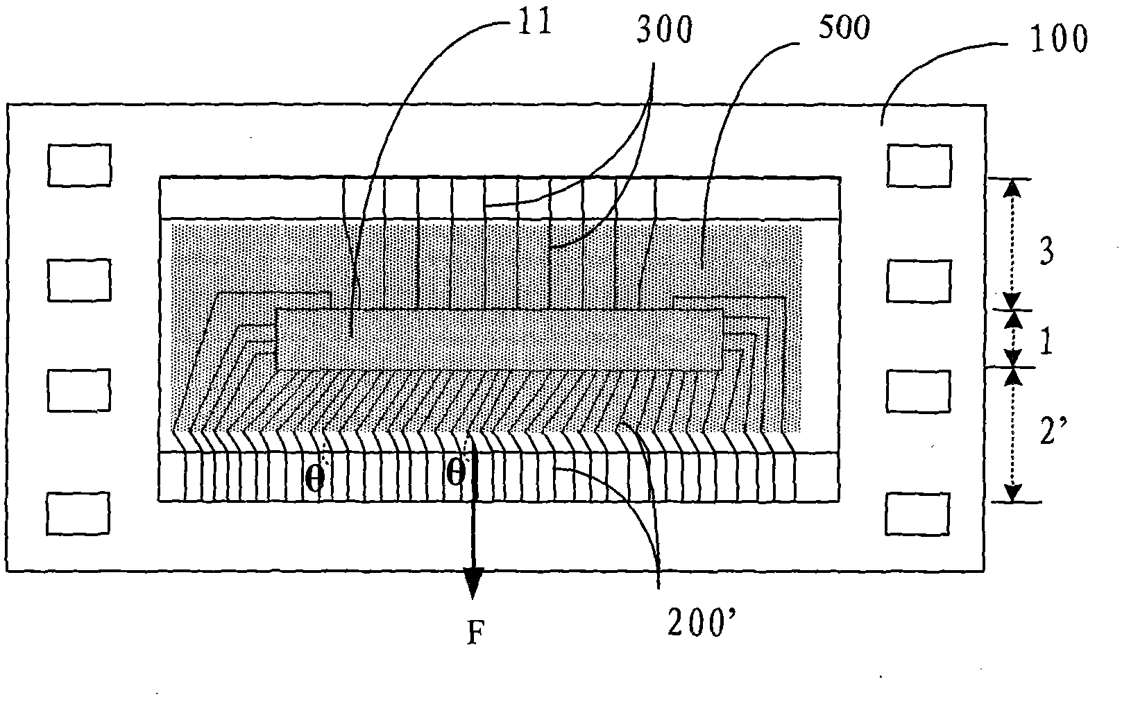
[0019] Please also refer to image 3 and Figure 4 , image 3 It is a schematic plan view of the first embodiment of the flexible printed circuit board of the flat panel display device of the present invention, Figure 4 It is a schematic diagram of crimping the flexible printed circuit board of the present invention on the array substrate. Such as image 3 and Figure 4 As shown, the flexible printed circuit board of the flat panel display device of the present invention is an element formed with various circuit patterns on the flexible substrate 100, and can be divided into a chip area 1, an array substrate side lead area 2' and a drive circuit board side lead area 3.

[0020] The chip area 1 includes a semiconductor chip 11 arranged on a flexible substrate 100, and the leads in the array substrate side lead ar...


PUM


Abstract

The invention discloses a flexible printed circuit board of a flat panel display device, comprising a chip region, an array substrate side lead region and a driving circuit board side lead region, wherein the array substrate side lead region has a crimping region, an S/R covering region and an exposing region; and leads in the exposing region and the crimping region have an included angle which is not zero or 180 degrees; and the included angle can be a obtuse angle capable of tapering from the middle to the two sides. The invention effectively solves the problem of lead cracking or fracturing due to stress by forming slant leads in the exposed region of the flexible printed circuit board so as to decrease the stress of the leads.

Description

technical field [0001] The invention relates to a flexible printed circuit board of a plane display device, in particular to a flexible printed circuit board of a plane display device which prevents lead wires from cracking. Background technique [0002] The flexible printed circuit board (Tape Package) of the flat-panel display device is a component with various circuit patterns formed on the flexible substrate, which is used to connect the drive circuit board to the array substrate of the liquid crystal panel. The flexible printed circuit board includes a tape carrier package (Tape Package) Carrier Package, hereinafter referred to as TCP) or Chip On Film (Chip On Film, hereinafter referred to as COF). Among them, TCP is thicker than COF and is not easy to bend, but the circuit structure of the two is roughly the same. [0003] The installation of the flexible printed circuit board of the flat panel display device mainly adopts an Outer Lead Bonding (OLB for short) method....

Claims


Application Information

Patent Timeline
Patent Type & Authority Applications(China)
IPC IPC(8): H05K1/02G02F1/133
Inventor 梁尚荣
Owner BOE TECH GRP CO LTD
Why Eureka
Try Eureka