Organic electroluminescent diode device
An electroluminescent layer, electroluminescent technology, applied in the direction of electric solid devices, electrical components, semiconductor devices, etc., can solve the problem of ITO film morphology, carrier transport and injection performance is difficult to control, the proportion of element indium is not suitable for control, and there are The performance of electroluminescent devices is unstable, and the effect of excellent carrier transport and injection performance and high light transmittance can be achieved.
- Summary
- Abstract
- Description
- Claims
- Application Information
AI Technical Summary
Problems solved by technology
Method used
Image
Examples
Embodiment 1
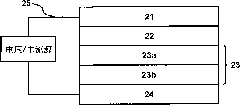
[0033] see figure 2 , the organic electroluminescent device has three structural layers: an anode 23 , an organic electroluminescent layer 22 and a cathode 21 ; their structural relationship is that the organic electroluminescent layer 22 is between the anode 23 and the cathode 21 . The anode 23 of the device is composed of two parts: a metal aluminum layer 23b and an aluminum oxide layer 23a, wherein the aluminum oxide layer 23a is between the metal aluminum layer 23b and the organic electroluminescent layer 22 . The thickness of the metal aluminum layer 23b is selected between 0.1nm and 200nm; the thickness of the aluminum oxide layer 23a formed on the metal aluminum layer 23b is between 0.1nm and 5nm. The organic electroluminescent layer 22 is formed on the aluminum oxide layer 23 a, and the cathode 21 is formed on the organic electroluminescent layer 22 . The anode and cathode of the organic electroluminescent device are connected to a power supply through an external ci...
Embodiment 2
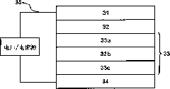
[0036] see image 3 , the organic electroluminescent device has three structural layers: an anode 33 , an organic electroluminescent layer 32 and a cathode 31 ; their structural relationship is that the organic electroluminescent layer 32 is between the anode 33 and the cathode 31 . The anode 33 of this device is made up of three parts: multilayer metal oxide layer 33a, aluminum oxide layer 33b and metal Al layer 33c; Their position relation is: aluminum oxide layer 33b is in multilayer metal oxide layer 33a and metal Al layer Between 33c. The organic electroluminescent layer 32 is sequentially formed on the multi-layer metal oxide layer 33 a, and the cathode 31 is formed on the organic electroluminescent layer 32 . The number of metal oxide layers 33a is between 1 and 10 layers, and the total thickness is between 0.1 nm and 1000 nm. The thickness of the aluminum oxide layer 33b is between 0.1nm and 5nm. The total thickness of the metal aluminum layer 33c is between 0.1nm a...
PUM
| Property | Measurement | Unit |
|---|---|---|
| thickness | aaaaa | aaaaa |
| thickness | aaaaa | aaaaa |
| thickness | aaaaa | aaaaa |
Abstract
Description
Claims
Application Information


