Packaging substrate and chip packaging structure

A chip packaging structure and packaging substrate technology, applied in electrical components, electrical solid-state devices, circuits, etc., can solve problems such as labor-intensive, wrong pin-finding, eye-consuming and time-consuming

Inactive Publication Date: 2011-09-21
CHIPMOS TECH INC
View PDF0 Cites 0 Cited by
  • Summary
  • Abstract
  • Description
  • Claims
  • Application Information

AI Technical Summary

Problems solved by technology

[0007] However, there are hundreds of pins at every turn, and analysts need to spend their eyesight and time to concentrate on calculating one by one to find out the pins corresponding to the abnormal test data.
This is not only labor-intensive, but also inefficient, and it is easier to find the wrong pin due to a wrong number, resulting in twice the result with half the effort

Method used


Image

  • Packaging substrate and chip packaging structure
  • Packaging substrate and chip packaging structure
  • Packaging substrate and chip packaging structure

Examples


Embodiment Construction

[0018] The invention provides a packaging substrate and a chip packaging structure comprising the packaging substrate. Several specific embodiments according to the present invention are disclosed as follows.

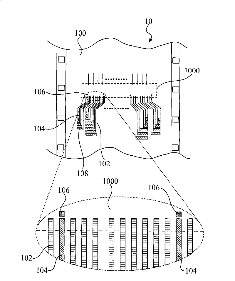
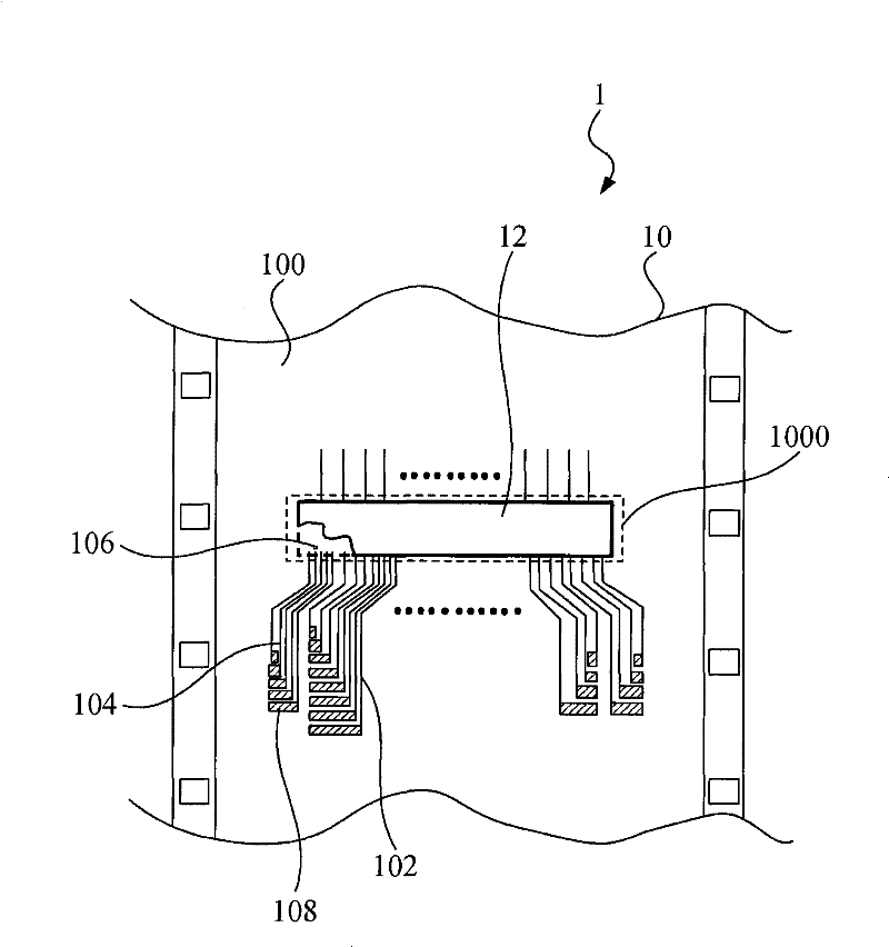
[0019] Please also refer to figure 1 as well as figure 2 , figure 1 A top view of a packaging substrate 10 according to a specific embodiment of the present invention is shown; figure 2 A top view of the chip package structure 1 according to an embodiment of the present invention is shown (wherein the chip 12 is partially shown in perspective). As shown in the figure, the chip package structure 1 of the present invention includes the package substrate 10 and a chip 12 disposed on the package substrate 10 .

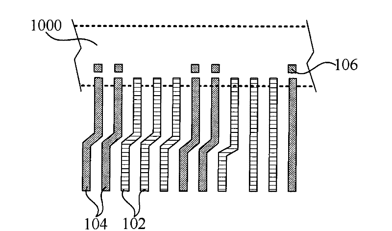
[0020] further, such as figure 1 and figure 2 As shown, the package substrate 10 of the present invention includes a flexible dielectric layer 100 , a plurality of first leads 102 , a plurality of second leads 104 , a plurality of marks 106 and a plurality ...


PUM


Abstract

The invention provides a package substrate and a chip packaging structure. The package substrate can be used for carrying a chip and comprises a flexible dielectric layer, a plurality of first pins, a plurality of second pins and a plurality of marks, wherein the flexible dielectric layer is provided with a chip bonding area used for arranging the chip; the first pins and the second pins are arranged on the flexible dielectric layer and respectively extend outward from the chip bonding area; the marks are positioned in the chip bonding area and arranged on the flexible dielectric layer in correspondence to the second pins; each M second pins in the second pins form a second pin group; the first pins are positioned among all second pin groups; and the M is a positive integer.

Description

technical field [0001] The present invention relates to a packaging substrate and a chip packaging structure including the packaging substrate, and in particular, the packaging substrate according to the present invention includes a plurality of marks corresponding to some pins, so that users can easily calculate the number of pins, Then quickly find the position of the pin you are looking for. Background technique [0002] With the advancement of semiconductor technology and the improvement of user needs, more and more electronic products need to use high-performance chips as the computing core. The improvement of chip performance usually also means the increase of the number and types of signals input to or output by the chip. Therefore, the number of pins or wires used for signal transmission also needs to be greatly increased. [0003] However, since the volume or size of most electronic products themselves or their components tends to be thinner or miniaturized, the ch...

Claims


Application Information

Patent Timeline
Patent Type & Authority Patents(China)
IPC IPC(8): H01L23/498H01L23/544
Inventor 李明勋沈弘哲
Owner CHIPMOS TECH INC
Why Eureka
Try Eureka