Image sensor and method of fabricating same

A technology of image sensing and manufacturing method, applied in radiation control devices, semiconductor/solid-state device manufacturing, electrical components, etc., to achieve the effect of reducing optical crosstalk and improving performance

Active Publication Date: 2010-10-06
TAIWAN SEMICON MFG CO LTD
View PDF0 Cites 23 Cited by
  • Summary
  • Abstract
  • Description
  • Claims
  • Application Information

AI Technical Summary

Problems solved by technology

Therefore, the known manufacturing methods of image sensors can meet the general needs, but cannot fully meet the needs of various aspects.

Method used


Image

  • Image sensor and method of fabricating same
  • Image sensor and method of fabricating same
  • Image sensor and method of fabricating same

Examples


Embodiment Construction

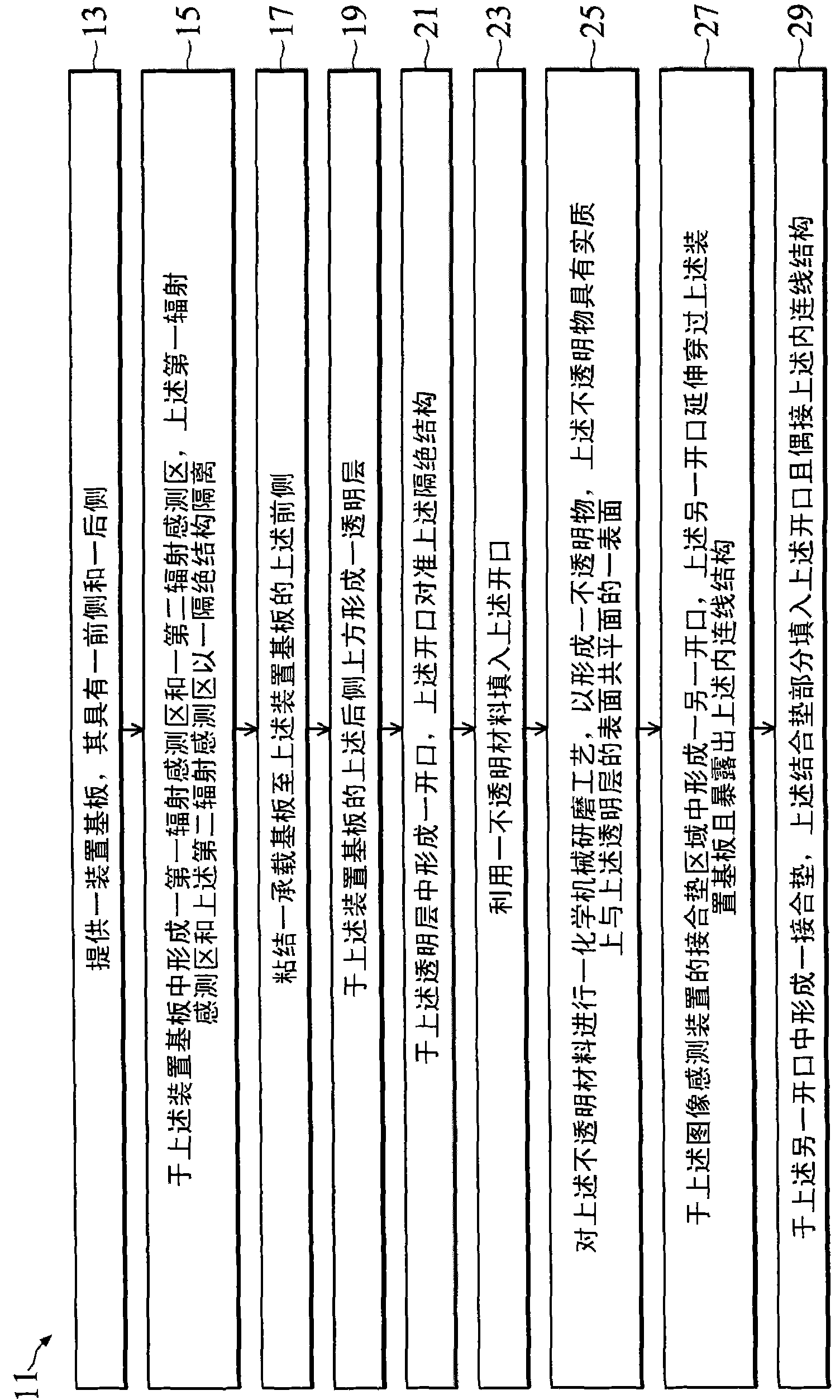
[0050] Hereinafter, each embodiment is described in detail and examples accompanied by accompanying drawings are used as a reference basis of the present invention. In the drawings or descriptions of the specification, the same reference numerals are used for similar or identical parts. And in the drawings, the shapes or thicknesses of the embodiments may be enlarged, and marked for simplicity or convenience. In addition, the parts of each element in the drawings will be described separately. It should be noted that the elements not shown or described in the drawings are forms known to those of ordinary skill in the art. In addition, specific embodiments only The specific method used in the present invention is disclosed, and it is not intended to limit the present invention.

[0051] figure 1 It is a process flow diagram of a method 11 for manufacturing a back-illuminated image sensor device (BSI image sensor device) according to an embodiment of the present invention. The ...


PUM


Abstract

Provided is a method of fabricating an image sensor device. The method includes providing a device substrate having a front side and a back side. The method includes forming first and second radiation-sensing regions in the device substrate, the first and second radiation-sensing regions being separated by an isolation structure. The method also includes forming a transparent layer over the back side of the device substrate. The method further includes forming an opening in the transparent layer, the opening being aligned with the isolation structure. The method also includes filling the opening with an opaque material. The invention can reduce the optical crosstalk in the image sensor device and can improve the performance of the image sensor device.

Description

technical field [0001] The invention relates to a semiconductor device, in particular to an image sensing device. Background technique [0002] Semiconductor image sensing devices are used to sense radiation such as light. Complementary metal-oxide-semiconductor transistor (CMOS) image sensors (CIS) and charge-coupled device (CCD) sensors are widely used in various applications such as digital video cameras or camera elements of mobile phones. These elements use a matrix of pixels in a substrate, which includes photodiodes and transistors that absorb radiation projected toward the substrate and convert the sensed radiation into electrical signals. However, an image sensor can generate a glitch signal when one pixel in the image sensor absorbs light that is intended to be projected toward another pixel. This interference signal can be regarded as optical cross-talk, and the optical cross-talk will degrade the performance of the image sensor. In addition, the image sensor m...

Claims


Application Information

Patent Timeline
Patent Type & Authority Applications(China)
IPC IPC(8): H01L21/82H01L21/3205H01L27/146
CPCH01L27/14636H01L27/14685H01L27/1463H01L27/14623H01L27/1464
Inventor 王文德杨敦年刘人诚庄俊杰林政贤
Owner TAIWAN SEMICON MFG CO LTD
Why Eureka
Try Eureka