
Double-color infrared detector and manufacturing method thereof
A technology for infrared detectors and manufacturing methods, which is applied in the fields of electric radiation detectors, semiconductor devices, and final product manufacturing, and can solve problems such as large crosstalk, large crosstalk, and easy diffusion of few births
- Summary
- Abstract
- Description
- Claims
- Application Information
AI Technical Summary
Problems solved by technology
Method used
Image


Examples
Embodiment 1
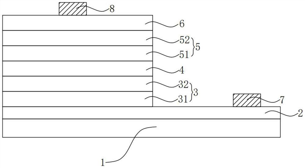
[0032] Such as figure 2 As shown, the n-type blue channel layer 3 in this embodiment includes an n-type blue channel absorbing layer 31 and an n-type blue channel barrier layer sequentially stacked on the first n-type contact layer 2 32. The n-type red channel layer 5 includes an n-type red channel barrier layer 51 and an n-type red channel absorbing layer 52 stacked on the p-type connection layer 4 in sequence. In this embodiment, the n-type blue channel absorbing layer 31 and the n-type red channel absorbing layer 52 are placed on both sides of the overall detector;
[0033] and if figure 2As shown, between the n-type blue channel absorbing layer 31 and the p-type connecting layer 4, and between the n-type red channel absorbing layer 52 and the p-type connecting layer 4, an n-type blue channel is respectively arranged. The color channel barrier layer 32 and the n-type red channel barrier layer 51, so that the n-type absorption layer, the n-type barrier layer and the p-t...
Embodiment 2
[0050] This embodiment specifically illustrates the manufacturing method of the two-color infrared detector of Embodiment 1.
[0051] Such as Figure 3 to Figure 6 As shown, the production method includes:
[0052] Step S1, providing an n-type substrate 1, the material of the n-type substrate 1 is n-type InAs, the thickness is 500 μm, and the doping concentration is 5×10 16 cm -3 .
[0053] Step S2, using a metal-organic chemical vapor deposition (MOCVD) process as a growth process, and the growth sources are TMGa, TMIn, TMSb and AsH 3 , the n-type dopant source is SiH 4 , the p-type dopant source is DEZn, the growth temperature is about 600°C, and the reaction chamber pressure is 200Torr. After the impurities on the surface of the n-type substrate 1 are removed by high-temperature treatment, the first n-type contact layer 2, the n-type blue channel absorption layer 31, and the n-type blue channel absorption layer 31 are sequentially formed on the n-type substrate 1. Cha...
Embodiment 3
[0066] This embodiment specifically illustrates another manufacturing method of the two-color infrared detector of Embodiment 1.
[0067] Such as Figure 3 to Figure 6 As shown, the production method includes:
[0068] Step S1, providing an n-type substrate 1, the material of the n-type substrate 1 is n-type GaSb, the thickness is 500 μm, and the doping concentration is 2×10 18 cm -3 .
[0069]Step S2, using molecular beam epitaxy (MBE) as the growth process, the growth source is solid elemental source In, As and Sb, the n-type dopant source is Si, the p-type dopant source is Be, and the growth temperature is about 400°C. After the impurities on the surface of the n-type substrate 1 are removed by high-temperature treatment, the first n-type contact layer 2, the n-type blue channel absorption layer 31, and the n-type blue channel absorption layer 31 are sequentially formed on the n-type substrate 1. Channel barrier layer 32, p-type connection layer 4, n-type red channel ba...
PUM
| Property | Measurement | Unit |
|---|---|---|
| Thickness | aaaaa | aaaaa |
| Doping concentration | aaaaa | aaaaa |
| Thickness | aaaaa | aaaaa |
Abstract
Description
Claims
Application Information