

Pixel isolation structure and manufacturing method of pixel isolation structure
A pixel isolation and isolation structure technology, applied in semiconductor/solid-state device manufacturing, radiation control devices, electrical components, etc., can solve problems such as optical crosstalk that cannot be solved
- Summary
- Abstract
- Description
- Claims
- Application Information
AI Technical Summary
Problems solved by technology
Method used
Image

Examples
no. 1 example
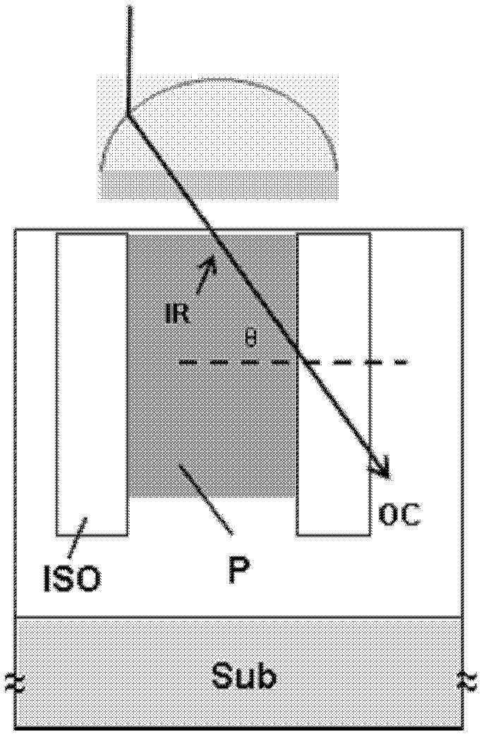
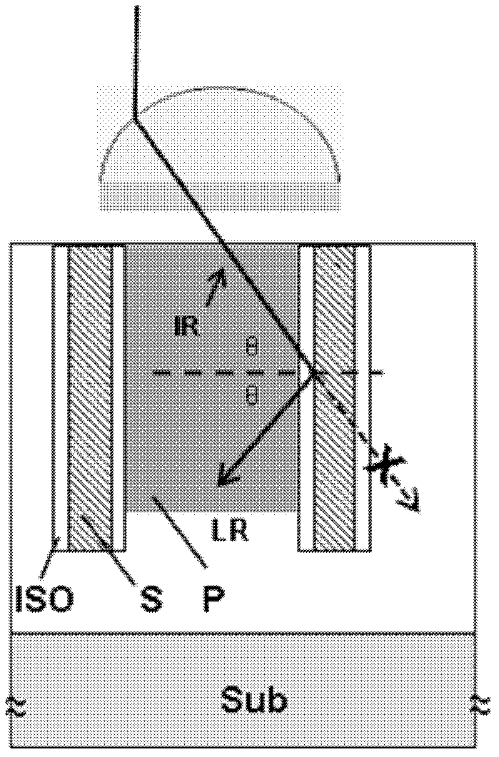
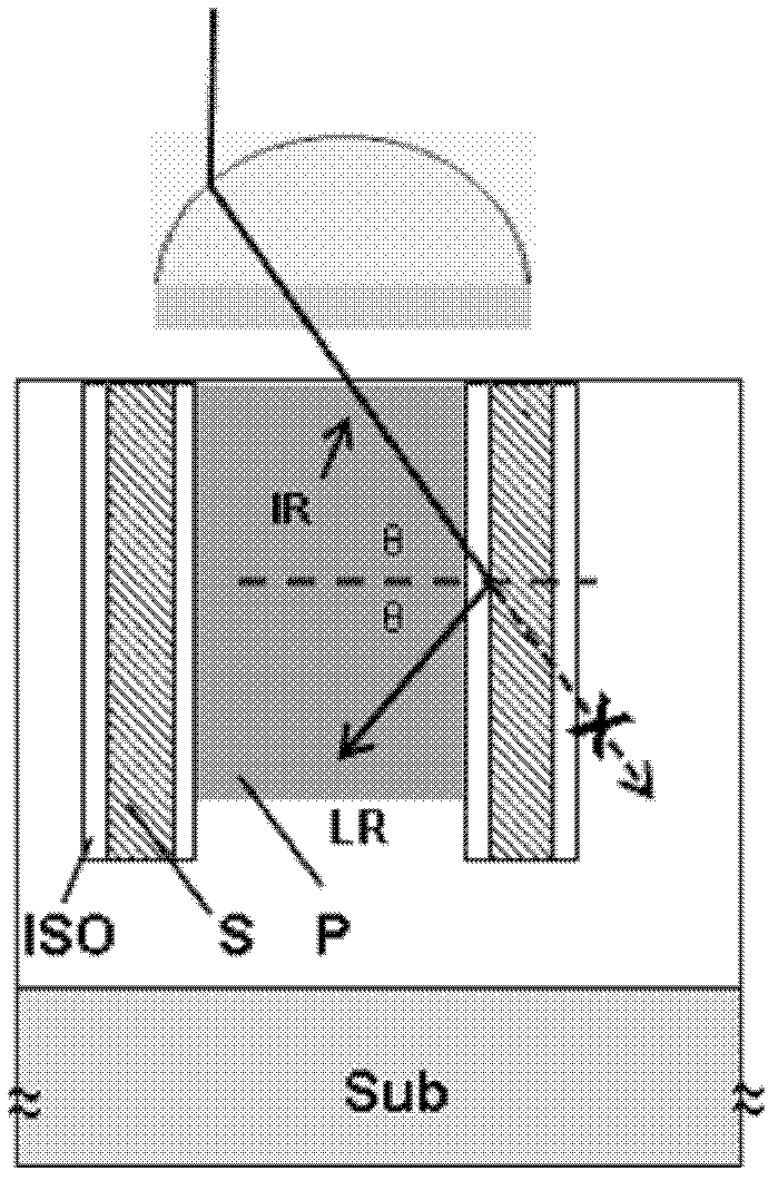
[0024] figure 2 A pixel isolation structure according to an embodiment of the present invention is schematically shown.
[0025] Such as figure 2 As shown, the pixel structure P according to the embodiment of the present invention is arranged on the substrate Sub, and the isolation structure ISO is arranged around the pixel structure P. Also, an oxide layer S is arranged in the isolation structure ISO.
[0026] Preferably, the oxide layer S is a silicon dioxide layer. Also, the silica layer had a refractive index of 1.4.
[0027] Further, as figure 2 As shown, when the incident light IR that enters the pixel structure P at an incident angle θ through various optical elements and reaches the isolation structure ISO after passing through a certain distance in the pixel structure P, the incident light IR will enter the isolation structure ISO and reach the isolation structure ISO. The interface between the structure ISO and the oxide layer S.
[0028] At this time, due t...
no. 2 example
[0031] Next, a method for manufacturing a pixel isolation structure according to an embodiment of the present invention will be described.
[0032] First, a pixel structure and an isolation structure may be arranged on a substrate such that the isolation structure is arranged around the pixel structure.
[0033] Subsequently, boron doping is performed on the isolation structure.
[0034] Finally, an oxide layer, for example a silicon dioxide layer with a refractive index of 1.4, is formed in the isolation structure by oxygen implantation.
PUM
 Abstract
Description
Claims
Application Information