Organic EL device, EL display panel, method for manufacturing the organic EL device and method for manufacturing the EL display panel

A technology for electroluminescent devices and manufacturing methods, applied in the fields of organic light-emitting device manufacturing/processing, organic light-emitting devices, electroluminescent light sources, etc., capable of solving problems such as rising surface impedance, short-circuiting of organic EL devices, and rising driving voltage of organic EL devices, etc. problems, achieve the effects of reducing surface impedance, high luminous efficiency, and improving yield

Active Publication Date: 2010-10-06
JOLED INC
View PDF1 Cites 27 Cited by
  • Summary
  • Abstract
  • Description
  • Claims
  • Application Information

AI Technical Summary

Problems solved by technology

However, since the hole transport layer made of metal oxide is dissolved by alkali or water, for example, it may be dissolved during the formation of the bank by etching with an alkali solution, and the surface of the hole transport layer may become deformed. uneven
When the surface of the hole transport layer is uneven, the work function of the hole transport layer is not constant, and the luminous efficiency of the organic EL device may decrease.
In addition, when the hole transport layer is dissolved by an alkaline solution, the surface roughness of the hole transport layer may increase.
If the surface roughness of the hole transport layer increases, it will be difficult for the functional layer formed on the hole transport layer to cover the entire surface of the hole transport layer, so that the organic EL device may be short-circuited.
[0009] In addition, when banks are formed after the formation of the hole transport layer, the surface of the hole transport layer may be contaminated by residues from the banks.
If the surface of the hole transport layer is contaminated by the residue of the bank, the efficiency of the hole transport layer will further vary, and the luminous efficiency of the organic EL device may decrease.
In addition, since the bank is an insulator, after the surface of the hole transport layer is polluted by the residue of the bank, the surface impedance of the hole transport layer increases, and the driving voltage of the organic EL device increases.

Method used


Image

  • Organic EL device, EL display panel, method for manufacturing the organic EL device and method for manufacturing the EL display panel
  • Organic EL device, EL display panel, method for manufacturing the organic EL device and method for manufacturing the EL display panel
  • Organic EL device, EL display panel, method for manufacturing the organic EL device and method for manufacturing the EL display panel

Examples


Embodiment approach 1

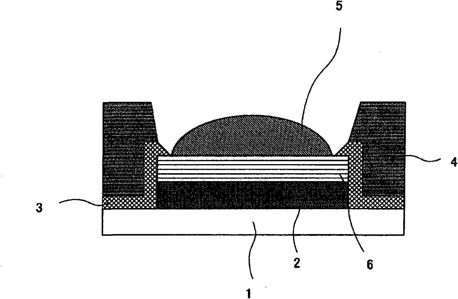
[0148] In Embodiment 1, a top emission type organic EL device will be described.

[0149] Figure 5 It is a cross-sectional view of the organic EL device 10 according to Embodiment 1 of the present invention.

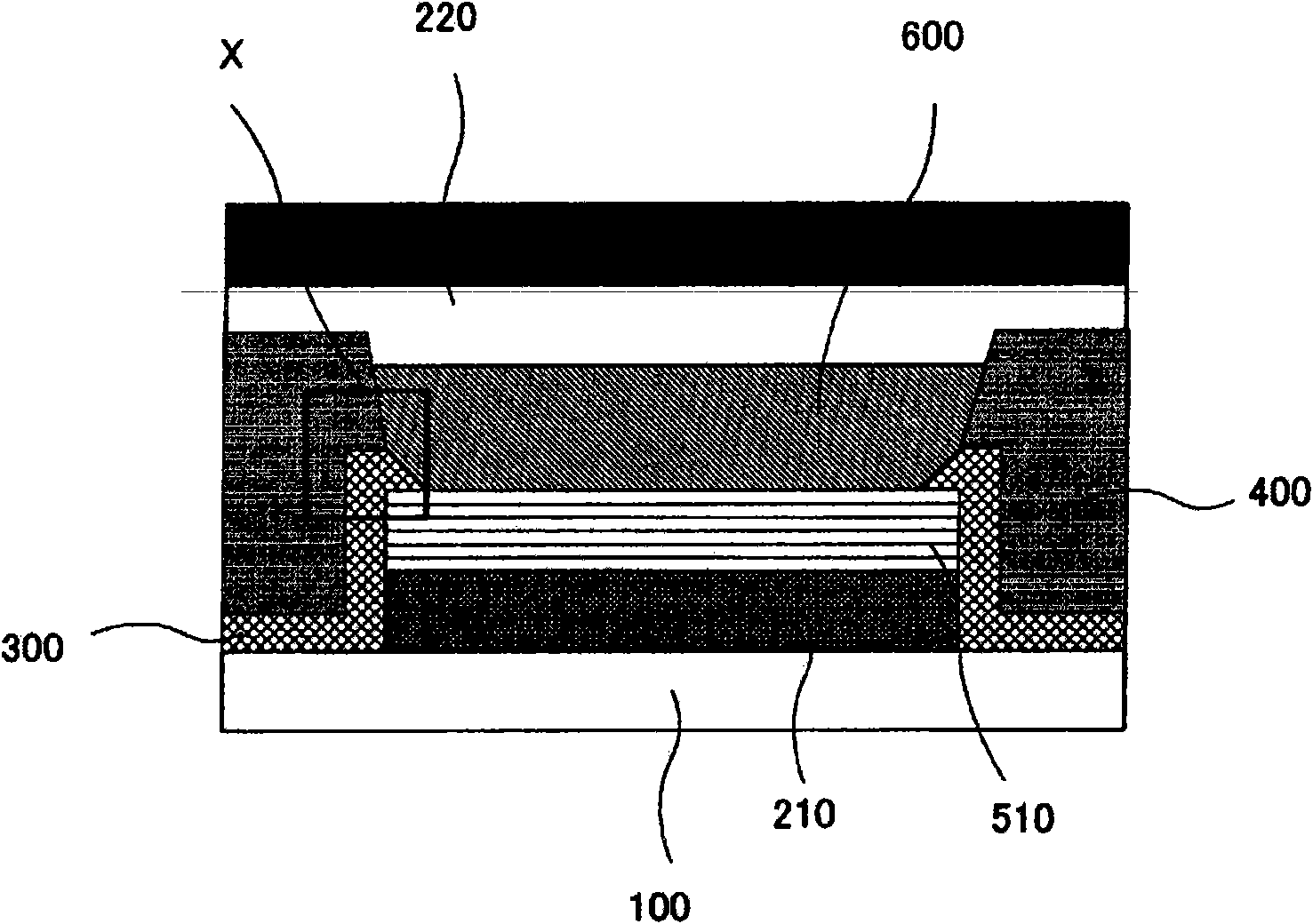
[0150] Figure 5 The organic EL device 10 includes: a substrate 100 , a reflective anode 210 , a hole transport layer 510 , an intermediate layer 520 , an organic light-emitting layer 600 , an inorganic film 300 , a bank 400 , a transparent cathode 220 and a sealing film 700 .

[0151] The substrate 100 is, for example, a glass plate.

[0152] The reflective anode 210 is a conductive layer disposed on the substrate 100 . Reflective anode 210 is made of, for example, APC alloy. The reflective anode 210 preferably has a thickness of 100 nm to 200 nm.

[0153] The hole transport layer 510 is disposed on the reflective anode 210 . The hole transport layer 510 is made of tungsten oxide (WOx). The thickness of the hole transport layer 510 is preferably 20 nm to 50 nm. ...

Embodiment approach 2

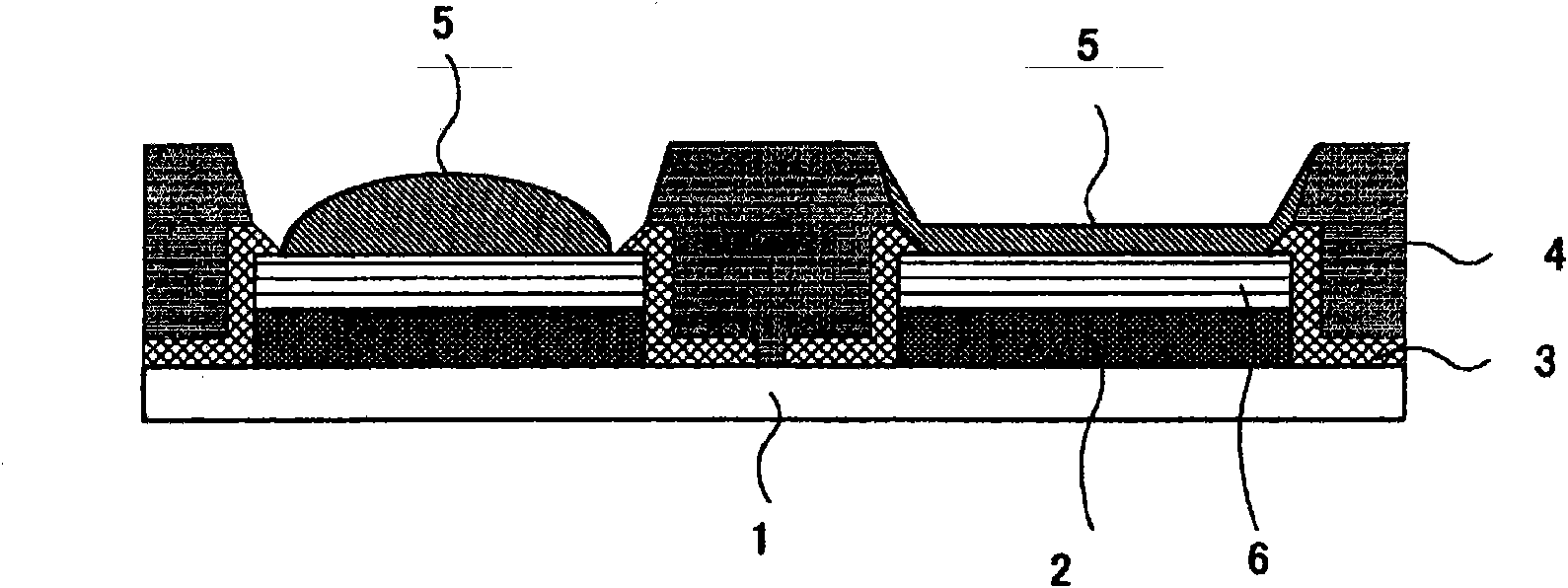
[0174] In Embodiment 1, an organic EL device in which a hole transport layer is in contact with an inorganic film is described. On the other hand, in Embodiment Mode 2, an organic EL device in which a hole transport layer and an inorganic film are separated will be described.

[0175] Figure 7 It is a cross-sectional view of the organic EL device 20 of the second embodiment. exist Figure 7 Among them, the organic EL device 20 includes: a substrate 100, a reflective anode 210, a hole transport layer 510, an intermediate layer 520, an organic light emitting layer 600, an electron transport layer 530, a transparent cathode 220, a sealing film 700, a bank 400, and an inorganic film 300 .

[0176] The materials of the substrate 100, the reflective anode 210, the inorganic film 300, the hole transport layer 510, the intermediate layer 520, the organic light-emitting layer 600, the transparent cathode 220, the sealing film 700, and the banks 400 may be the same as those describe...

Embodiment approach 3

[0182] As described in Embodiment Mode 1 and Embodiment Mode 2, the hole transport layer of the present invention is preferably an oxide of a transition metal, but the material of the hole transport layer of the present invention may also be PEDOT-PSS (doped with Polyethylenedioxythiophene of polystyrene sulfonic acid) When the material of the hole transport layer is PEDOT-PSS, the present invention can protect the surface of the anode from being polluted by the residue of the bank.

[0183] In Embodiment 3, an example in which the material of the hole transport layer is PEDOT-PSS (polyethylenedioxythiophene doped with polystyrenesulfonic acid) will be described. Figure 9 It is a cross-sectional view of the organic EL device 30 according to Embodiment 3 of the present invention.

[0184] Figure 9 The organic EL device 30 includes: a substrate 100 , a transparent anode 210 , a hole transport layer 510 , an intermediate layer 520 , an organic light-emitting layer 600 , an ino...


PUM


Abstract

Disclosed is a method for manufacturing an organic EL device which comprises a hole injection layer having a flat surface that is not contaminated. Specifically disclosed method for manufacturing an organic EL device, which comprises a step of forming an anode on a substrate; a step of forming a hole injection layer on the anode; a step of forming an inorganic film on the substrate and the hole injection layer; a step of forming a bank on the inorganic film in such a manner that at least a part of the inorganic film formed on the hole injection layer is exposed; a step of etching the exposed inorganic film by using the bank as a mask so that the hole injection layer is exposed therefrom; and a step of forming an organic light-emitting layer by applying an organic light-emitting material onto the exposed hole injection layer. The hole injection layer contains tungsten oxide or molybdenum oxide.

Description

technical field [0001] The present invention relates to an organic EL (Electroluminescent: electroluminescence) device, an organic EL display panel and a manufacturing method thereof. Background technique [0002] In recent years, research and development on self-luminous displays typified by organic EL displays have been actively conducted as candidates for post-liquid crystal displays and post-plasma displays. There are two types of current organic EL displays. One is a low-molecular-weight organic EL display using a low-molecular-weight organic compound in a light-emitting layer, and the other is a high-molecular-weight organic EL display using a high-molecular organic compound. [0003] Currently, due to the high luminous efficiency and long life of the material, the development of low-molecular-weight organic EL displays that use vacuum processes such as vacuum evaporation to produce the light-emitting layer is in the lead. However, the organic light-emitting layer of...

Claims


Application Information

Patent Timeline
Patent Type & Authority Applications(China)
IPC IPC(8): H01L51/50H01L29/786H01L51/05H05B33/10H05B33/22
CPCH01L51/56H01L51/0025H01L51/0059H01L27/3246H01L2251/308H01L51/0029H01L51/5088H10K59/122H10K71/311H10K71/811H10K85/631H10K50/17H10K2102/103H10K71/00
Inventor 中谷修平吉田英博
Owner JOLED INC
Why Eureka
Try Eureka