Check patentability & draft patents in minutes with Patsnap Eureka AI!

LED packaging module capable of releasing stress

A LED packaging, self-release technology, applied in electrical components, circuits, semiconductor devices, etc., can solve the problems of gold wire impact, open circuit, stress can not be effectively released, etc., to reduce abnormal damage, alleviate rapid temperature rise, improve use effect of life

Inactive Publication Date: 2012-11-21
FOSHAN INST SUN YAT SEN UNIV
View PDF1 Cites 0 Cited by
  • Summary
  • Abstract
  • Description
  • Claims
  • Application Information

AI Technical Summary

Problems solved by technology

On the one hand, the accumulated heat will cause temperature rise, the working environment of the LED chip will deteriorate, and the light will decay prematurely. On the other hand, the internal stress of the sealant will be generated due to thermal expansion and contraction. Since the sealant is in a fully enclosed structure, The stress cannot be effectively released, and the stress will impact the gold wire, and the probability of breaking the gold wire or gold wire solder joints is greatly increased. Often, the circuit breaks when the package module has not reached its service life, and the module cannot be used intermittently.

Method used


Image

  • LED packaging module capable of releasing stress
  • LED packaging module capable of releasing stress
  • LED packaging module capable of releasing stress

Examples


Embodiment Construction

[0021] The present invention will be described in further detail below with reference to the accompanying drawings.

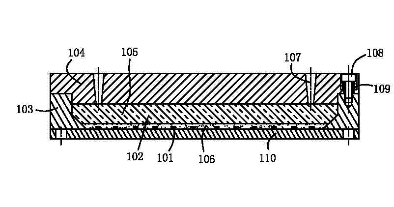
[0022] reference figure 1 , The first embodiment of the present invention is a self-relieving LED package module, including an LED chip 101, the LED chip 101 is arranged at the bottom of a cavity 102, the top of the cavity 102 has an opening, the opening An optical plate 104 is provided; the optical plate 104 and the cavity 102 form a closed accommodating space; the accommodating space is provided with a soft glue 105; the optical plate 104 can be directed to the outside of the accommodating space Move in order to release the stress generated by the heat of the soft rubber 105, which is specifically realized by the structure described above. The outer side wall (referring to the part that extends into the cavity) of the optical plate 104 and the inner side wall of the cavity 102 With a clearance fit, the optical plate 104 and the cavity 102 can move due to the the...


PUM


Abstract

The invention relates to the semiconductor illumination technology, in particular to an LED packaging module, comprising an LED wafer. The LED packaging module is characterized in that the LED wafer is arranged at the bottom of a cavity, the top of the cavity is provided with an opening, the opening is provided with an optical plate, the optical plate and the cavity form a closed accumulating space in which flexible glue is arranged, and the optical plate can move or deform towards the outer side of the accumulating space so as to release the thermal stress of the flexible glue.

Description

Technical field [0001] The invention relates to semiconductor lighting technology, in particular to an LED package module. Background technique [0002] Traditional LED packaging technology generally uses a lens to seal the LED chip and encapsulant to form a package module or light source. [0003] Chinese patent document CN101369614 discloses a high-power white light emitting diode packaging structure and packaging method on February 18, 2009, which mainly include LED chips, substrates, inner sealing gel, phosphor layer or phosphor gel layer, and outer sealing lens. It is characterized in that the LED chip is attached to the substrate, the chip electrode is connected to the circuit layer on the substrate, the LED chip is covered by an inner sealant, and the outer surface of the inner sealant is covered by a phosphor layer or a phosphor adhesive layer. Or the outer surface of the phosphor glue layer is covered by the outer sealing lens. [0004] Just like the structure disclosed in...

Claims


Application Information

Patent Timeline
Patent Type & Authority Patents(China)
IPC IPC(8): H01L33/52H01L33/56
Inventor 王钢罗滔
Owner FOSHAN INST SUN YAT SEN UNIV
Features
  • R&D
  • Intellectual Property
  • Life Sciences
  • Materials
  • Tech Scout
  • Unparalleled Data Quality
  • Higher Quality Content
  • 60% Fewer Hallucinations
Learn More