MOS structure for inhibiting SOI floating-body effect and manufacturing method thereof

A technology of MOS structure and floating body effect, applied in semiconductor devices, semiconductor/solid-state device manufacturing, electrical components, etc., can solve the problems of reducing body potential, increasing device area, and increasing parasitic effects

Inactive Publication Date: 2010-10-27
SHANGHAI INST OF MICROSYSTEM & INFORMATION TECH CHINESE ACAD OF SCI
View PDF0 Cites 4 Cited by
  • Summary
  • Abstract
  • Description
  • Claims
  • Application Information

AI Technical Summary

Problems solved by technology

For SOI PMOS, due to the relatively low ionization rate of holes, the electron-hole pairs generated by impact ionization are much lower than that of SOI NMOS, so the Kink effect in SOI PMOS is not obvious
[0005] In order to solve the partially depleted SOI NMOS, the body contact method is usually used to connect the "body" to a fixed potential (source or ground), such as Figure 1a-1b As shown, it is a traditional T-shaped gate structure contact, and the P formed at one end of the T-shaped gate + The injection region is connected to the P-type body region under the gate. When the MOS device is working, the carriers accumulated in the body region pass through the P-type body region. + Channel bleed to achieve the purpose of reducing the potential of the body region. The negative effect is to complicate the process flow, increase the parasitic effect, reduce some electrical properties and increase the device area.

Method used


Image

  • MOS structure for inhibiting SOI floating-body effect and manufacturing method thereof
  • MOS structure for inhibiting SOI floating-body effect and manufacturing method thereof
  • MOS structure for inhibiting SOI floating-body effect and manufacturing method thereof

Examples


Embodiment 1

[0025] This embodiment provides a method for fabricating a MOS structure that suppresses the floating body effect, such as image 3 shown, including the following steps:

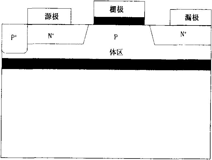
[0026] First, a shallow trench isolation structure 300 is formed on the semiconductor material (SOI or GOI, etc.) with a buried insulating layer 200, the active area is isolated, and P ion implantation is performed in the active area; then, a mask is added , the mask is opened at the position of the first conductivity type source region 401, and heavily doped P ions are implanted vertically through the mask to form a heavily doped P-type region; then the gate dielectric layer 501 and the gate electrode 500 are fabricated, Lightly doped source region (LDS) and lightly doped drain region (LDD) are performed, and finally N ion implantation is performed in the source region and the drain region to form the first conductivity type source region 401 and the first conductivity type drain region 402, between them A...

Embodiment 2

[0028] This embodiment provides another method for fabricating a MOS structure that suppresses the floating body effect, such as Figure 4 shown, including the following steps:

[0029]First, a shallow trench isolation structure 300 is fabricated on the semiconductor material (SOI or GOI, etc.) with a buried insulating layer 200, the active area is isolated, and P ion implantation is performed in the active area; then the gate dielectric layer 501, The gate electrode 500 is lightly doped in the source region (LDS) and lightly doped in the drain region (LDD); then, a mask is added, and the mask is opened at the position of the source region 401 of the first conductivity type, through the mask Perform heavily doped P ion implantation vertically to form a heavily doped P-type region under the lightly doped source region (LDS); finally perform N ion implantation in the source region and drain region to form the first conductivity type source region 401 and The drain region 402 of...

Embodiment 3

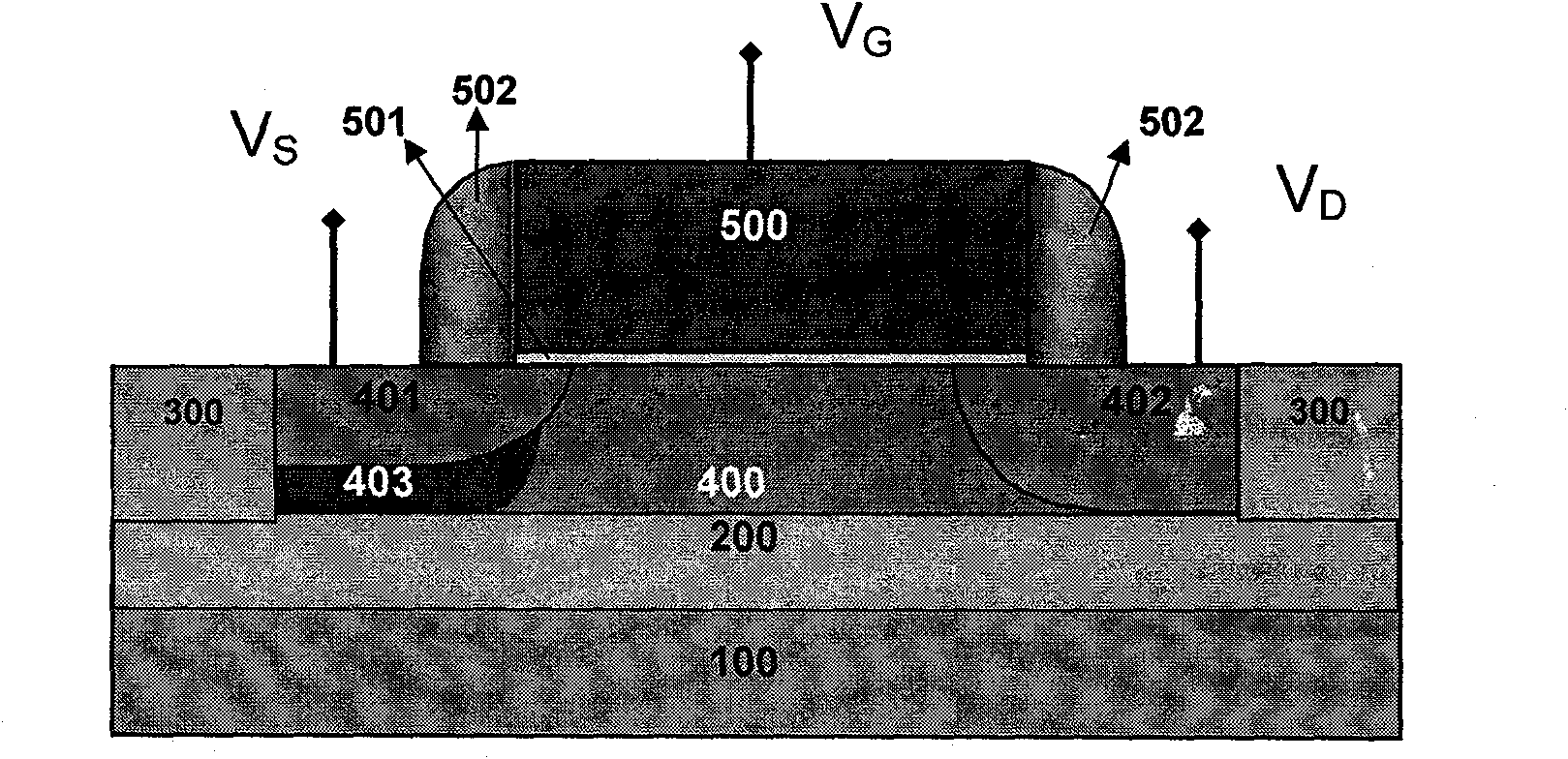
[0031] This embodiment provides a third method of fabricating a MOS structure that suppresses the floating body effect, such as Figure 5 As shown, the method forms a body region 400, a first conductivity type source region 401 and a first conductivity type drain respectively located at both ends of the body region 400 on a semiconductor material (SOI or GOI, etc.) having a buried insulating layer 200. region 402, and the gate region (gate dielectric layer 501, gate electrode 500, insulator dielectric spacer isolation structure 502) located on the body region 400, add a mask plate, through the mask plate to the first The conductivity type source region 401 is vertically implanted with ions, so that the region below the source region 401 and above the buried insulating layer 200 forms a heavily doped second conductivity type region 403 .

[0032] In order to analyze the performance of the MOS structure of the present invention, the structure is simulated, and the simulation res...


PUM


Abstract

The invention discloses an MOS structure for inhibiting SOI floating-body effect. The MOS structure comprises a substrate, a buried insulating layer positioned above the substrate and an active region positioned above the buried insulating layer, wherein the active region comprises a body region, and a first conduction type source region and a first conduction type drain region which are positioned at the two ends of the body region, and a heavily doped second conduction type region positioned between the first conduction type source region and the buried insulating layer; and a gate region is formed above the body region. When the structure is manufactured, the position of the first conduction type source region is subjected to ion implantation by a mask to make a region positioned on the lower part of the first conduction type source region and above the buried insulating layer form the heavily doped second conduction type region. The MOS structure inhibits the floating-body effect effectively, and has the advantages of no increase of chip area, compatibility of a manufacturing process with the conventional CMOS process and the like.

Description

technical field [0001] The invention relates to a MOS (Metal Oxide Semiconductor) structure and a manufacturing method thereof, in particular to a MOS structure capable of effectively suppressing the SOI floating body effect and a manufacturing method thereof, belonging to the technical field of semiconductor manufacturing. Background technique [0002] SOI (Silicon On Insulator) refers to silicon-on-insulator technology. In SOI technology, the device is only manufactured in a very thin silicon film on the surface, and the device and the substrate are separated by a buried oxide layer. It is this structure that makes SOI technology have the incomparable advantages of bulk silicon. The small parasitic capacitance enables SOI devices to have high speed and low power consumption. The full dielectric isolation of SOI CMOS devices completely eliminates the parasitic latch-up effect of bulk silicon CMOS devices, and SOI full dielectric isolation makes SOI technology have high int...

Claims


Application Information

Patent Timeline
Patent Type & Authority Applications(China)
IPC IPC(8): H01L21/74H01L21/336H01L29/78
CPCH01L29/1087H01L21/266H01L29/66772H01L29/78612H01L29/78624
Inventor 陈静罗杰馨伍青青肖德元王曦
Owner SHANGHAI INST OF MICROSYSTEM & INFORMATION TECH CHINESE ACAD OF SCI
Why Eureka
Try Eureka