Circuit and method for realizing TDI in CMOS image sensor

An image sensor, MOS tube technology, applied in the direction of image communication, TV, electrical components, etc., can solve problems such as limiting the application of TDI technology, and achieve the effect of expanding the scope of application

Active Publication Date: 2010-11-10
南通南平电子科技有限公司
View PDF5 Cites 30 Cited by
  • Summary
  • Abstract
  • Description
  • Claims
  • Application Information

AI Technical Summary

Problems solved by technology

[0006] In the prior art, there is no suitable circuit and method that can better implement TDI technology in CMOS image sensors, which limits the application of TDI technology

Method used


Image

  • Circuit and method for realizing TDI in CMOS image sensor
  • Circuit and method for realizing TDI in CMOS image sensor
  • Circuit and method for realizing TDI in CMOS image sensor

Examples


Embodiment Construction

[0034] In order to make the object, technical solution and advantages of the present invention clearer, the implementation manner of the present invention will be further described in detail below in conjunction with the accompanying drawings.

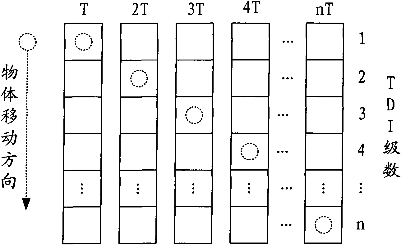
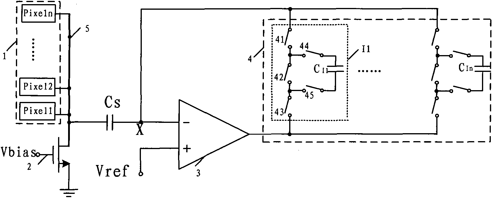
[0035] In order to better realize the TDI technology in the CMOS image sensor, an embodiment of the present invention provides a circuit for realizing TDI in the CMOS image sensor, see figure 2 , see the description below:

[0036] The circuit includes: an integrator array 4 composed of a pixel array 1, a MOS transistor 2, a sampling capacitor Cs, an operational amplifier 3, a column bus 5 and a plurality of integrators I1-In connected in parallel, and each integrator includes: a first switch 41, The second switch 42, the third switch 43, the fourth switch 44, the fifth switch 45 and the integrating capacitor;

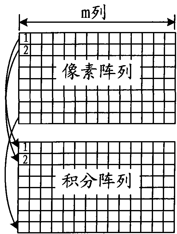
[0037] The pixel array 1 is respectively connected to one end of the sampling capacitor Cs and the source of the MOS transi...


PUM


Abstract

The invention discloses a circuit and a method for realizing a transport driver interface (TDI) in a complementary metal oxide semiconductor (CMOS) image sensor, and relates to the field of analog integrated circuit designs. The circuit comprises a pixel array, a metal oxide semiconductor (MOS) tube, a sampling capacitor, an operational amplifier, serial buses and an integrator array formed by connecting a plurality of integrators in parallel; each integrator comprises a first switch, a second switch, a third switch, a fourth switch, a fifth switch and an integrating capacitor; the pixel array is respectively connected with one end of the sampling capacitor and the source electrode of the MOS tube through serial buses; the grid electrode of the MOS tube is connected with a bias voltage; the drain electrode of the MOS tube is earthed; the other end of the sampling capacitor is respectively connected with the negative polarity end of the operational amplifier and one end of the first switch; the positive polarity end of the operational amplifier is connected with a reference voltage; the other end of the first switch is respectively connected with one end of the second switch and one end of the fourth switch; the other end of the second switch is respectively connected with one end of the third switch and one end of the fifth switch; the other end of the third switch is connected with the output end of the operational amplifier; the other end of the fourth switch is connected with one end of the integrating capacitor; and the other end of the integrating capacitor is connected with the other end of the fifth switch.

Description

technical field [0001] The invention relates to the field of analog integrated circuit design, in particular to a circuit and method for realizing TDI in a CMOS image sensor. Background technique [0002] TDI (Time Delay Integration, Time Delay Integration) technology is a technology that can increase the sensitivity of line array image sensors. It uses its special scanning method to achieve high sensitivity and signal-to-noise by making multiple exposures to the same target. Ratio, especially suitable for shooting occasions with low illumination and moving objects. The basic principle of TDI is to take multiple exposures of the same moving object and accumulate them. Since the photoreceptor accumulates multiple incident light, the image signal and the overall brightness will be greatly improved accordingly. [0003] CCD (Charge Coupled Device, Charge Coupled Device) image sensor is an ideal device for realizing TDI technology, and it can realize signal accumulation withou...

Claims


Application Information

Patent Timeline
Patent Type & Authority Applications(China)
IPC IPC(8): H04N5/335H04N3/15
Inventor 高静徐江涛史再峰叶颖聪
Owner 南通南平电子科技有限公司
Why Eureka
Try Eureka