Automatic optical inspection method for printed circuit board comprising resistance element

A technology of automatic optical inspection and printed circuit board, which is applied in the direction of material analysis, measuring devices, scientific instruments, etc. through optical means, and can solve problems such as poor promotion ability

Inactive Publication Date: 2010-12-15
SOUTH CHINA UNIV OF TECH
View PDF1 Cites 40 Cited by
  • Summary
  • Abstract
  • Description
  • Claims
  • Application Information

AI Technical Summary

Problems solved by technology

Although the neural network method has the advantage of self-learning, it requires a large number of samples for learning. When the number of samples is limited, it is easy to show poor generalization ability

Method used


Image

  • Automatic optical inspection method for printed circuit board comprising resistance element
  • Automatic optical inspection method for printed circuit board comprising resistance element
  • Automatic optical inspection method for printed circuit board comprising resistance element

Examples


Embodiment Construction

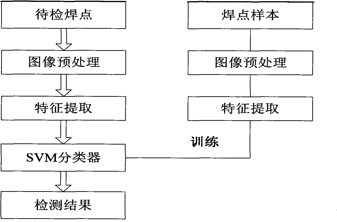
[0045] The flow chart of the method for detecting solder joints with resistance elements on printed circuit boards of the present invention is as attached figure 1 shown. Specifically, preprocessing and feature selection are performed on the solder joint image of the training sample first. After completing these two parts, the features of the solder joint image are input into the classifier for training. Finally, the same preprocessing and feature selection are performed on the solder joint image of the test sample, and the The test sample features are input into the classifier for classification.

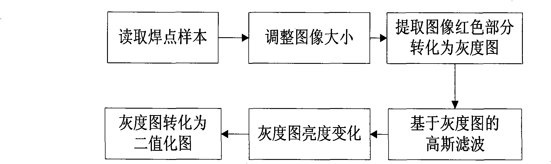
[0046] Such as figure 2 Shown is the solder joint image preprocessing flow chart. Since the size of the solder joint sample images is inconsistent, after inputting the image, all the solder joint images can be adjusted to the same length and width, so that it is easy to extract relevant features and information through standardized images . Then extract the red area and turn i...


PUM


Abstract

The invention relates to an automatic optical inspection method for a printed circuit board comprising a resistance element. After the characteristics of welding spots are extracted, the welding spots are correctly classified into three types of normality, starved solder and missing parts through a classifier of a support vector machine. The automatic optical inspection method is suitable for classification and detection of the special welding spots during production. The automatic optical inspection method comprises the following steps of: converting red areas in welding spot images into a grayscale image and a binary image; calculating grayscale image-based mean values and standard deviations, and binary image-based height-lightness ratio, cross correlation and area of area color; and classifying the welding spots according to the quality by using the mean values, the variance, the height-lightness ratio and the similarity level of the welding spot images in the classifier of the support vector machine. Wrong welding spot types are classified through the mean values, the variance, the height-lightness ratio and the area characteristics of the welding spots. After the quality of the welding spots is distinguished, the wrong welding spots can be further classified into two types of starved solder and missing parts by the method.

Description

technical field [0001] The invention relates to an automatic optical detection method for a resistive element in a printed circuit board. technical background [0002] Solder joint inspection techniques are mainly divided into two categories: destructive testing and nondestructive testing. Since non-destructive testing does not cause damage to original parts or products, it is of great help to improve production efficiency and reduce testing costs, and has become more and more mainstream technology today. Non-destructive testing methods mainly include: electrical testing, X-ray testing, automatic optical inspection (AOI). Among them, AOI is an application of computer vision, which can effectively detect the quality of solder joints, and has the advantages of real-time, rapidity, and high precision, and is also the detection technology used in the present invention. [0003] Several commonly used AOI algorithms used in printed circuit board solder joint detection are: templ...

Claims


Application Information

Patent Timeline
Patent Type & Authority Applications(China)
IPC IPC(8): G01N21/956G06T7/00
Inventor 高红霞麦倩胡跃明
Owner SOUTH CHINA UNIV OF TECH
Why Eureka
Try Eureka