
CMOS image sensor pixel sampling method

An image sensor and pixel technology, applied in image communication, TV, color TV components, etc., can solve problems such as pixel color errors

Active Publication Date: 2010-12-15
BEIJING SUPERPIX MICRO TECHNOLOGY CO LTD
View PDF11 Cites 8 Cited by
  • Summary
  • Abstract
  • Description
  • Claims
  • Application Information

AI Technical Summary

Problems solved by technology

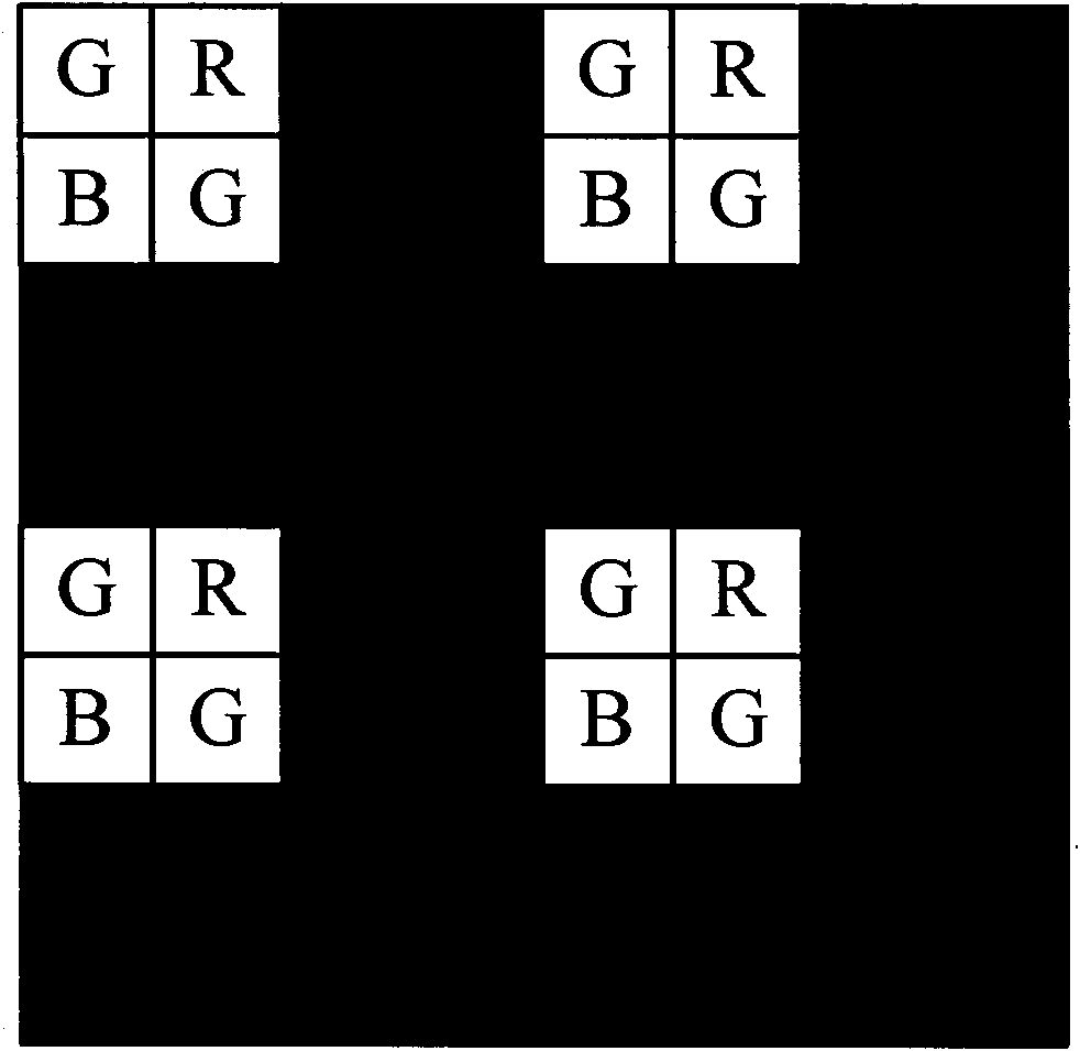
If this method is applied to realize 3 / 4 sampling value, the sampling result is as follows Figure 4 As shown, the last sampled pixel color is wrong

Method used


Image

  • CMOS image sensor pixel sampling method
  • CMOS image sensor pixel sampling method
  • CMOS image sensor pixel sampling method

Examples


specific Embodiment 1

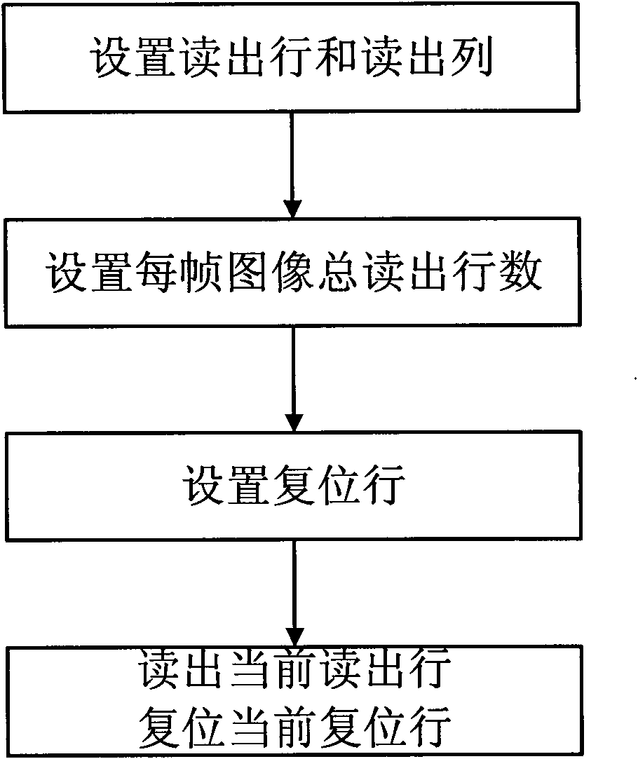
[0040] In this embodiment, an image sensor with a size of 1216 rows×1928 columns is taken as an example, the row number and column number are both counted from 0, and the pixel sampling value is 6 / 8 (2×3 / 2 3 ), that is, 3 / 4 sampling.

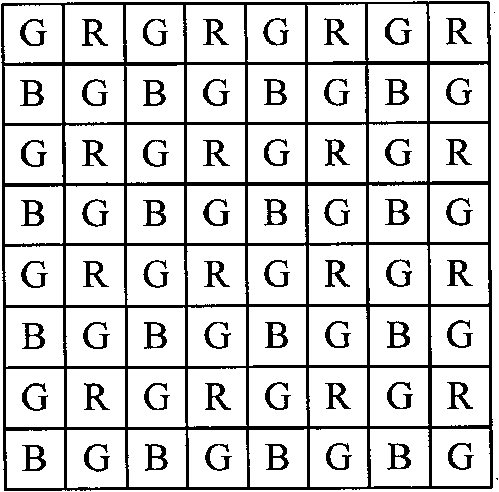
[0041] Because most of the color CMOS image sensors adopt the Bayer pattern mode, the color sequence is as follows: figure 2 shown. In order to maintain the color order of the image, 3 / 4 sampling can only be achieved by outputting 6 rows every 8 rows and 6 columns every 8 columns. Divide the serial numbers of all rows and columns by 8 and take the remainder. According to the result, it can be known that all row numbers and column numbers are between 8n~8n+7. If 3 / 4 sampling is realized, only the data of 8n+2~8n+7 rows needs to be read out, and the data of 8n~8n+1 rows are discarded. Similarly, only data in columns 8n+2 to 8n+7 is read in each read row.

[0042] The column counter will skip 8n and 8n+1 columns during the counting of the colum...


PUM


Abstract

The invention discloses a CMOS image sensor pixel sampling method, comprising the following steps of: firstly, sampling reading rows and reading columns through arranging an image sensor; arranging the total number of the reading rows of each frame; secondly, arranging reset rows through a calculation formula; and finally, reading the current reading rows and resetting the current reset rows according to the calculated result. In the image sensor pixel sampling way, reading row pixels and reading column pixels are selected according to a sampling value, meanwhile, non-reading rows are reset to realize irregular value pixel sampling, which breaks through the limitation which must sample according to the 1 / 2n traditional sampling value. The sampling method which enables the number of row pixels and the number of column pixel of output images of the CMOS image sensor to be reduced to 2m / 2n times of the original number of the row pixels and the number of the column pixels is adopted, the frame rate can be improved so that all reading rows are correctly exposed sequentially and the color correctness of the output images is ensured.

Description

technical field [0001] The invention relates to a pixel sampling method, in particular to a CMOS image sensor pixel sampling method. Background technique [0002] Benefiting from the development of semiconductor technology and the advancement of image processing technology, the image quality of CMOS image sensors has been greatly improved. With the development of information, communication, Internet and portable electronic equipment, CMOS image sensors are not only widely valued in the fields of mobile terminals and electronic handheld or imaging equipment, but also in mobile phones, camcorders, digital cameras including digital SLR cameras. Facing a rapidly growing market, CMOS image sensors have entered a period of rapid development. [0003] When the user integrates the CMOS image sensor into various devices, it usually requires it to be able to output reduced images of various resolutions, and thus the frame rate should be increased as the image resolution is reduced. ...

Claims


Application Information

Patent Timeline
IPC IPC(8): H04N3/15H04N5/335
Inventor 赵晓海程杰刘志碧陈杰唐冕
Owner BEIJING SUPERPIX MICRO TECHNOLOGY CO LTD
Learn More