

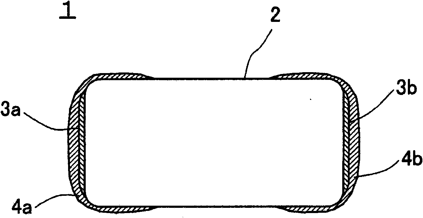
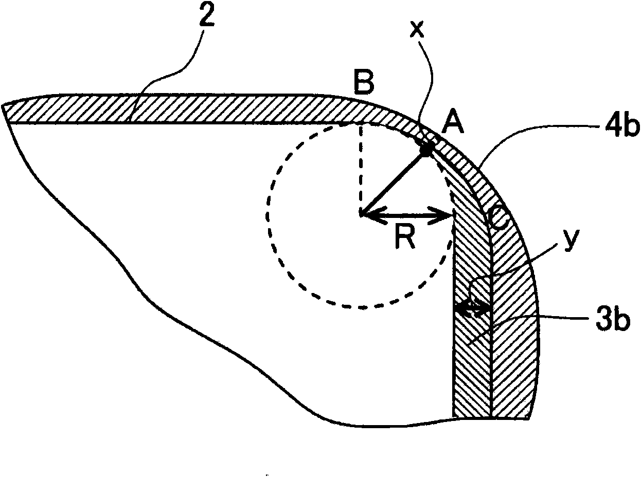
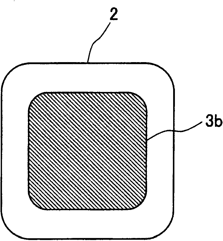
Chip-type semiconductor ceramic electronic component
一种电子元器件、半导体的技术,应用在电气元件、电阻器零部件、电阻器等方向,达到减小偏差、增大连接面积、减小电阻变化的效果
- Summary
- Abstract
- Description
- Claims
- Application Information
AI Technical Summary
Problems solved by technology
Method used
Image

Examples
Embodiment 1
[0063] First, prepare BaCO 3 , PbO, SrCO 3 , CaCO 3 , TiO, Er as a semiconducting agent 2 o 3 , Mn as a characteristic improver 2 o 3 , SiO as a sintering aid 2 As the starting material, and prepare the starting material shown in Table 1 and weighed according to the proportion shown in the following formula.
[0064] ((Ba, Pb, Sr, Ca) 0.0096 Er 0.004 ) TiO 3 +0.0005MnO 2 +0.02SiO2 2
[0065] Next, add pure water to various weighed starting materials, mix and pulverize them together with PSZ balls in a ball mill, after drying, pre-fire at 1150°C for 2 hours, and then pulverize them together with PSZ balls in a ball mill again to obtain Burnt powder. Next, an acrylic organic binder, a dispersant, and water were added to the obtained calcined powder, mixed with PSZ balls for 15 hours, granulated, and dried to obtain a ceramic raw material.
[0066] Then, the obtained ceramic raw material is used to form an unfired mother substrate, and after the binder is removed, t...
PUM
| Property | Measurement | Unit |
|---|---|---|
| radius | aaaaa | aaaaa |
Abstract
Description
Claims
Application Information