Preparation method of DMOS (Domplementary Metal Oxide Semiconductor) with self-aligned channel in BCD (Bipolar CMOS DMOS) process
A self-alignment and channel technology, applied in semiconductor/solid-state device manufacturing, electrical components, circuits, etc., can solve problems such as photoresist coating inhomogeneity
- Summary
- Abstract
- Description
- Claims
- Application Information
AI Technical Summary
Problems solved by technology
Method used
Image

Examples
Embodiment Construction
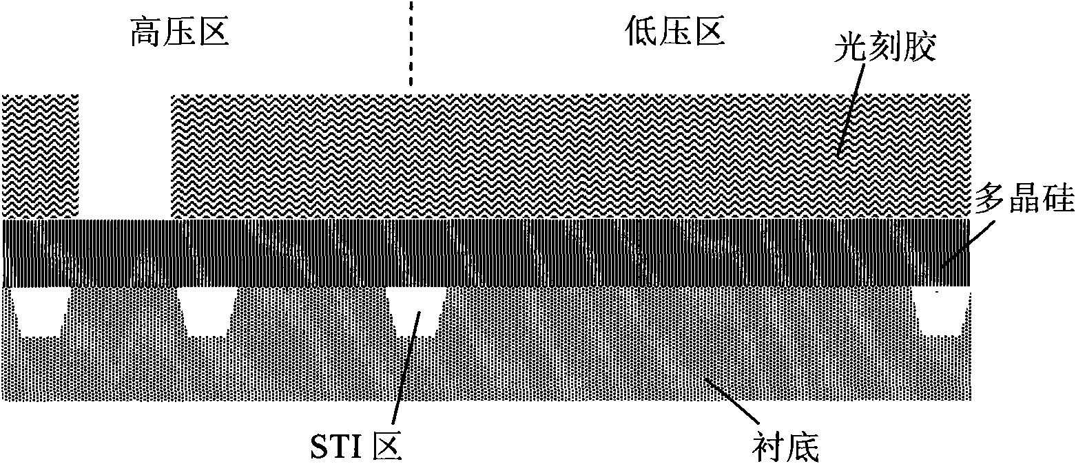
[0028] The preparation method of the DMOS of self-aligned channel in the BCD process of the present invention comprises the following steps (see figure 2 ):
[0029] 1) After the deposition of polysilicon is completed, the position of the source-drain injection region of the low-voltage region is defined by using a photolithography process (coating photoresist, then using a photolithography mask for photolithography, and then developing to form a photoresist pattern) , so that the polysilicon located in the source and drain implantation regions after photolithography is exposed, while other positions are covered by photoresist (see Figure 3a );
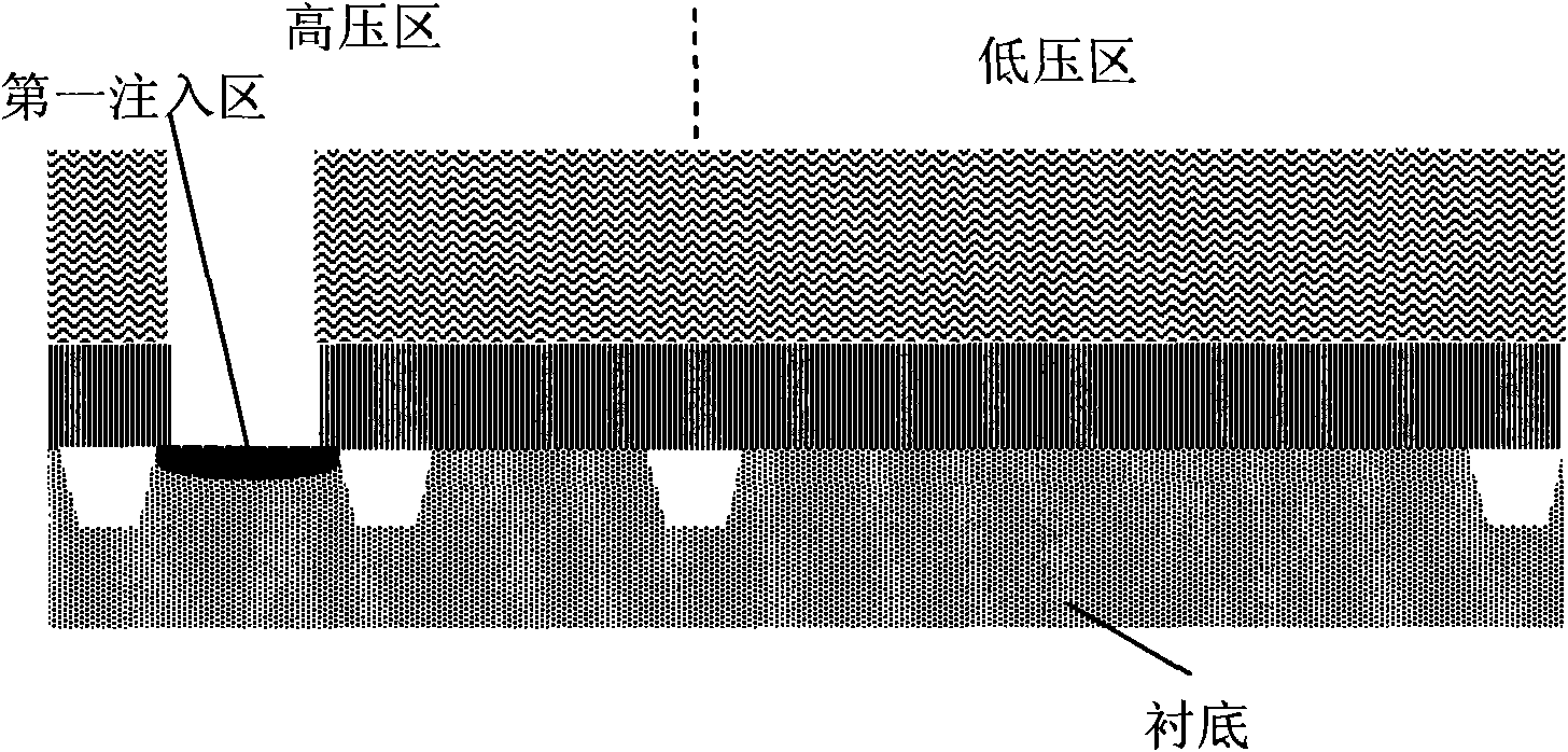
[0030] 2) Etching is located at the position of the source-drain injection region (that is, Figure 3i The position of the third implantation region shown in ) to the surface of the silicon substrate, after which the remaining photoresist is removed (see Figure 3b );
[0031] 3) Deposit an oxide liner layer on the surface of th...
PUM
 Abstract
Description
Claims
Application Information
 - R&D
- Intellectual Property
- Life Sciences
- Materials
- Tech Scout
- Unparalleled Data Quality
- Higher Quality Content
- 60% Fewer Hallucinations
Browse by: Latest US Patents, China's latest patents, Technical Efficacy Thesaurus, Application Domain, Technology Topic, Popular Technical Reports.
© 2025 PatSnap. All rights reserved.Legal|Privacy policy|Modern Slavery Act Transparency Statement|Sitemap|About US| Contact US: help@patsnap.com