Crystalline silicon solar cell

A technology of solar cells and crystalline silicon, applied in the field of solar cells, can solve the problems of reducing the utilization rate of incident light, affecting the conversion efficiency of cells, adversely affecting the conversion efficiency of cells, etc., and achieving the effects of improving injection efficiency, high conversion efficiency, and improving utilization rate

Active Publication Date: 2012-08-22
BEIJING NAURA MICROELECTRONICS EQUIP CO LTD
View PDF3 Cites 0 Cited by
  • Summary
  • Abstract
  • Description
  • Claims
  • Application Information

AI Technical Summary

Problems solved by technology

However, the problem is that the incident light hν enters the pn junction 3 through the grid line 4 to generate a photovoltaic effect to generate current. Due to the opacity of the silver material, when the grid line 4 is too dense, the grid line 4 covering the light-receiving surface will cause The effective light-receiving area of ​​the battery is reduced, and the utilization rate of incident light is reduced; and when the grid line 4 is too sparse, it cannot form a good ohmic contact with the n-type region 2, which will also affect the conversion efficiency of the battery
It can be seen that the grid line made of metal material is used as the cathode structure of the crystalline silicon solar cell, which hinders the cell from converting more light energy into electrical energy, which is not conducive to the improvement of cell conversion efficiency.

Method used


Image

  • Crystalline silicon solar cell
  • Crystalline silicon solar cell
  • Crystalline silicon solar cell

Examples


Embodiment 1

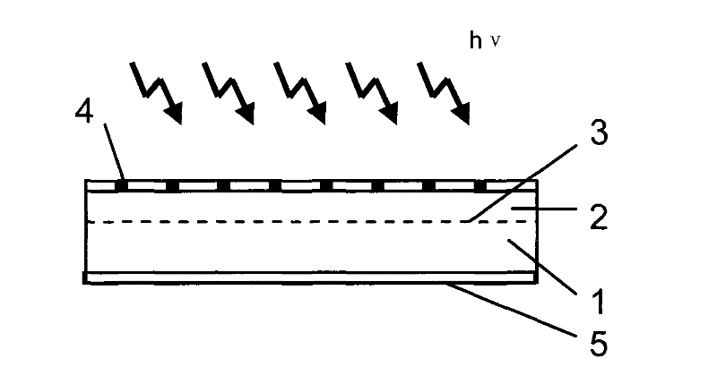
[0034] figure 2 This is a schematic diagram of the structure of the crystalline silicon solar cell in this embodiment.

[0035] Such as figure 2 As shown, crystalline silicon solar cells include:

[0036] p-type crystalline silicon substrate 12,

[0037] The n-type layer 13 on the substrate 12,

[0038] The cathode 14 on the n-type layer;

[0039] Wherein, the cathode 14 is a transparent conductive film, and its work function is less than or equal to 4.26 eV.

[0040] As a preferred technical solution, in this embodiment, the substrate 12 is composed of p-type crystalline silicon (single crystal silicon), and the thickness of the substrate 12 is in the range of 100-300 μm, preferably 220 μm in thickness, and the resistivity range is about It is 0.1-100 Ω·cm, and the resistivity is preferably 1.0 Ω·cm.

[0041] On the back light surface of the substrate 12, there is a metal aluminum electrode 11 made by a traditional process. The metal aluminum electrode 11 serves as the back electrode ...

Embodiment 2

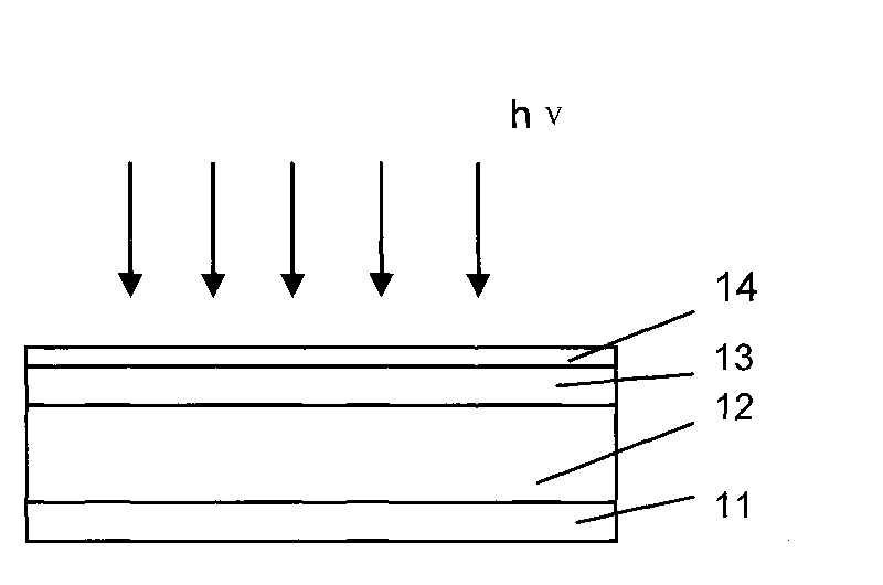
[0054] image 3 This is a schematic diagram of the structure of the crystalline silicon solar cell in this embodiment.

[0055] Such as image 3 As shown, crystalline silicon solar cells include:

[0056] p-type crystalline silicon substrate 22,

[0057] The n-type layer 23 on the substrate 22 is also a diffusion layer formed in a certain depth on the surface of the substrate 22,

[0058] The cathode 24 on the n-type layer has a metal back electrode 21 on the backlight surface of the substrate 22;

[0059] Wherein, the cathode 24 is a transparent conductive film, and its work function is less than or equal to 4.26 eV. Preferably, the transparent conductive film of the cathode 24 is LaB 6 , Deposited on the n-type layer by electron beam evaporation, LaB 6 The work function of the material is about 2.6~3.0eV, LaB 6 The thickness of the transparent conductive film ranges from 80 to 800 nm, and the thickness is preferably 250 nm.

[0060] The above is the same as the structure of the first ...

Embodiment 3

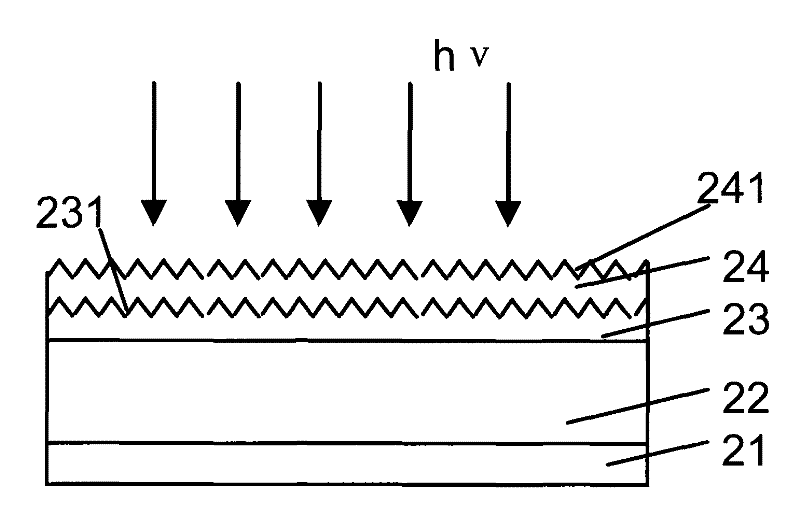
[0065] Figure 4 This is a schematic diagram of the structure of the crystalline silicon solar cell in this embodiment.

[0066] Such as Figure 4 As shown, crystalline silicon solar cells include:

[0067] p-type crystalline silicon substrate 32,

[0068] The n-type layer 33 on the substrate 32, the n-type layer 33 is doped thin film silicon,

[0069] The cathode 34 on the n-type layer;

[0070] Wherein, the cathode 34 is a transparent conductive film, and its work function is less than or equal to 4.26 eV. Preferably, the transparent conductive film of the cathode 34 is LaB6, which is deposited on the n-type layer by electron beam evaporation. The work function of the LaB6 material is about 2.6 to 3.0 eV. The thickness of the LaB6 transparent conductive film is in the range of 80 to 800 nm, and the preferred thickness is 250nm.

[0071] The difference between this embodiment and the previous embodiments is that an n-type doped thin film silicon layer is used instead of the n-type dif...


PUM


Abstract

The invention provides a crystalline silicon solar cell, which comprises a substrate of p-type crystalline silicon, an n-type layer on the substrate and a cathode on the n-type layer, wherein the cathode is a transparent conductive film with the work function less than or equal to 4.26eV; the transparent conductive film comprises LaB6 with the work function from 2.6 to 3.0eV; and the light transmittance of the transparent conductive film is 35 to 70 percent. The adoption of the transparent conductive film as the cathode of the cell makes it easy for sunlight to pass through the cathode to reach the pn junction to improve the utilization rate of the incident light so as to convert more luminous energy into electric energy. Furthermore, the work function of the transparent conductive film is at least not greater than that of metal silver, so the transparent conductive film can form excellent ohm contact with the n-type layer to improve the injection efficiency of electrons. Therefore, the crystalline silicon solar cell has higher conversion efficiency.

Description

Technical field [0001] The invention relates to the technical field of solar cells, in particular to a crystalline silicon solar cell. Background technique [0002] Since the introduction of practical solar cells in 1954, crystalline silicon solar cells have been dominating the world photovoltaic market, accounting for 80% to 90% of the total output of solar cells. In recent years, as the raw material cost of crystalline silicon has decreased, it is expected that this dominant position will continue to be maintained for a long period of time. [0003] In order not to be replaced by thin-film solar cells with cheaper advantages, the research and development of crystalline silicon solar cells are closely focused on improving cell conversion efficiency and reducing cell costs. At present, the main technical obstacles restricting the further improvement of the conversion efficiency of crystalline silicon solar cells include: ① the shading effect of the grid lines on the front surface ...

Claims


Application Information

Patent Timeline
Patent Type & Authority Patents(China)
IPC IPC(8): H01L31/042H01L31/0224
CPCY02E10/50
Inventor 胡立琼
Owner BEIJING NAURA MICROELECTRONICS EQUIP CO LTD
Why Eureka
Try Eureka