Supercharge Your Innovation With Domain-Expert AI Agents!

Output buffering circuit, amplifier device and display device

一种输出缓冲、显示装置的技术,应用在放大装置的零部件、放大器、带有半导体器件/放电管的放大器等方向,能够解决减短源极驱动芯片寿命等问题

Active Publication Date: 2011-03-30
HIMAX TECH LTD +1
View PDF4 Cites 9 Cited by
  • Summary
  • Abstract
  • Description
  • Claims
  • Application Information

AI Technical Summary

Problems solved by technology

On the other hand, due to the relatively large panel load and precise system specifications, the power loss is often worth considering. The power loss causes the source driver chip to overheat and shorten the life of the source driver chip.

Method used


Image

  • Output buffering circuit, amplifier device and display device
  • Output buffering circuit, amplifier device and display device
  • Output buffering circuit, amplifier device and display device

Examples


Embodiment Construction

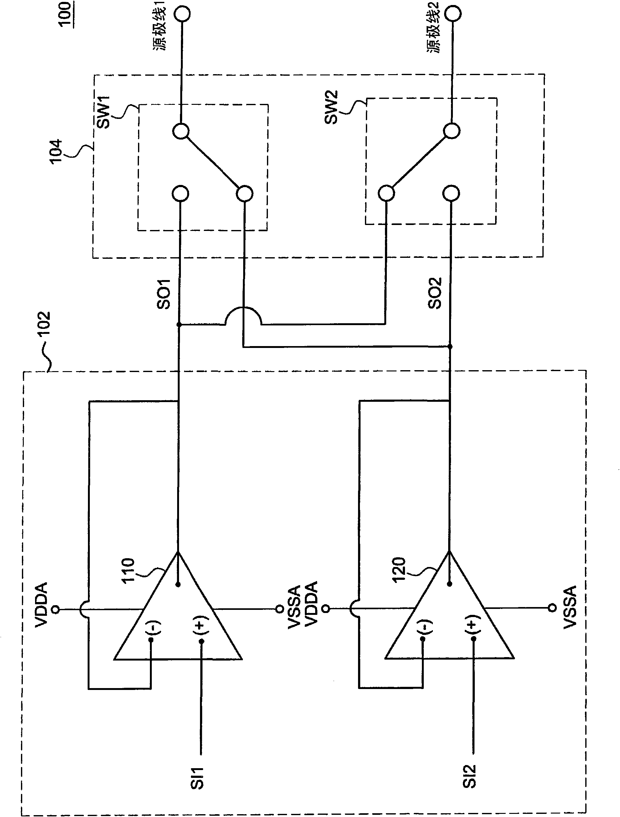
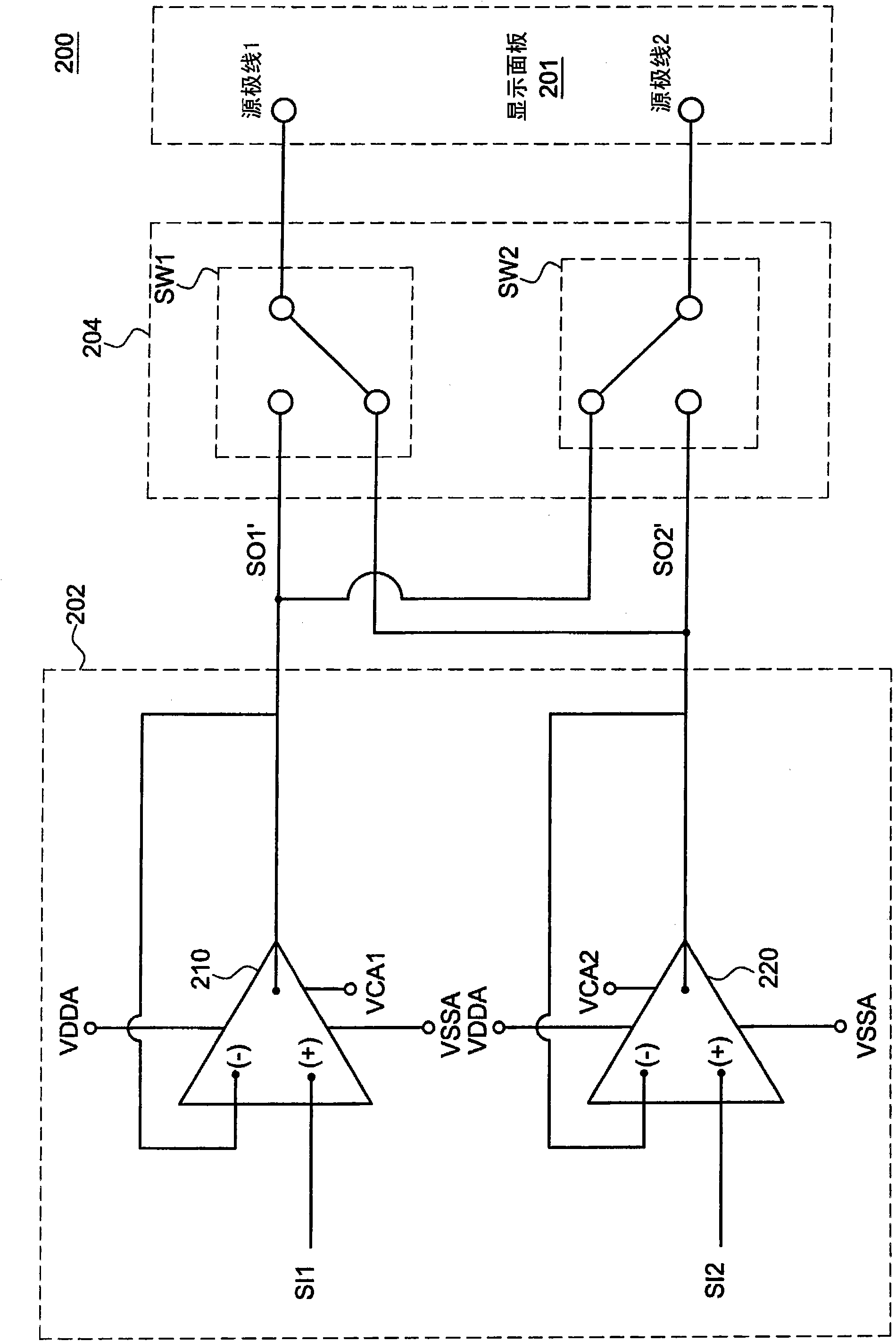
[0020] figure 2 It is a schematic diagram of an embodiment of the source driving device of the present invention, such as figure 2 As shown, a source driver 200 is assembled on the display panel 201 for driving the display panel 201 and includes an output buffer circuit 202 and a switch circuit 204 .

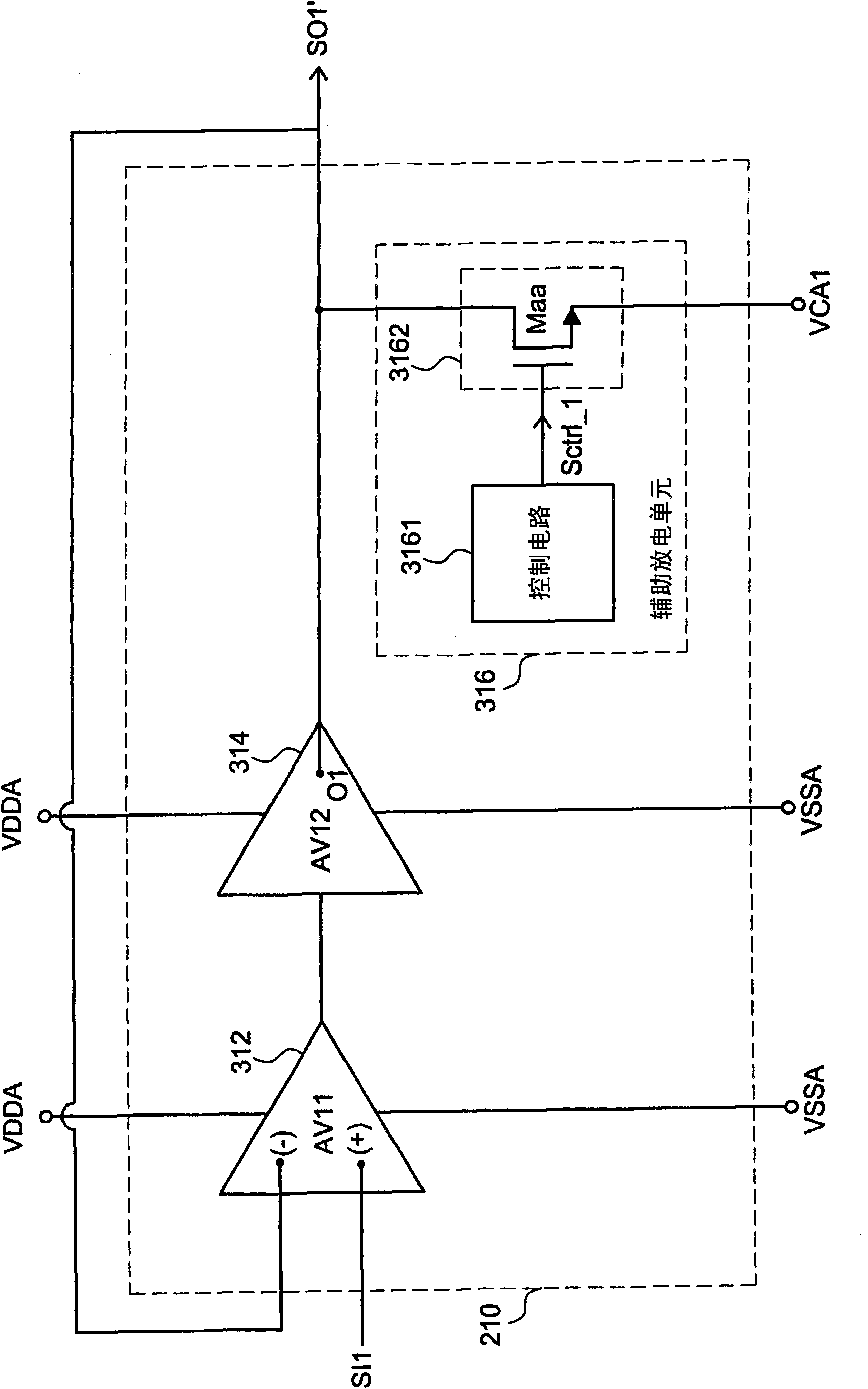
[0021] The output buffer circuit 202 includes a first amplifying circuit 210 and a second amplifying circuit 220 . The first amplifying circuit 210 can receive a first input signal SI1, for example, the first input signal SI1 can come from a D / A converter (not shown in the figure), and provide a first output according to the first input signal SI1 The signal SO1 ′ is used to drive the display panel 201 . Similarly, the second amplifying circuit 220 receives the second input signal SI2, and then provides a second output signal SO2' for driving the display panel 201 according to the second input signal SI2.

[0022] The switch circuit 204 controls the coupling relationship am...


PUM


Abstract

The present invention relates to an output buffering circuit, an amplifier device and a display device. The output buffering circuit includes first and second amplifier circuits. The first amplifier circuit includes a first input stage and a first output stage both coupled between a first power voltage and a second power voltage lower than the first power voltage, and an assistant discharging unit configured to provide a discharging current flowing from a first output node to a first intermediate power voltage during a discharging operation of the first amplifier circuit. The second amplifier circuit includes a second input stage and a second output stage both coupled between the first power voltage and the second power voltage, and an assistant charging unit configured to provide a charging current flowing from a second intermediate power voltage to a second output node during a charging operation of the second amplifier circuit. The first and second amplifier circuits can have reduced output voltage ranges and hence reduced total power consumption.

Description

technical field [0001] The invention relates to a display device, in particular to a driving device, an amplifier device and an output buffer circuit of the display device. Background technique [0002] Generally, a source driver chip of a display system includes hundreds of source driver circuits, and each source driver circuit is responsible for driving at least one source line of a panel of the display system. Therefore, the power loss of a single source driver circuit has a great impact on the entire source driver chip. A source drive circuit generally includes an output buffer circuit, and the output buffer circuit has a large impact on the overall power consumption and operating speed of the source drive circuit. For a portable electronic product, it consumes less power The output buffer circuit can prolong the life of the battery. On the other hand, due to the large size of the panel is relatively accompanied by the panel load and precise system specifications, so t...

Claims


Application Information

Patent Timeline
Patent Type & Authority Applications(China)
IPC IPC(8): G09G3/20
CPCH03F3/3022G09G3/2092H03F1/0205G09G2300/0426G09G2330/021G09G2360/18
Inventor 蔡建泓王家辉张进添陈英烈
Owner HIMAX TECH LTD
Features
  • R&D
  • Intellectual Property
  • Life Sciences
  • Materials
  • Tech Scout
  • Unparalleled Data Quality
  • Higher Quality Content
  • 60% Fewer Hallucinations
Learn More