

Method for manufacturing tungsten plunger
A manufacturing method and tungsten plugging technology, applied in semiconductor/solid-state device manufacturing, electrical components, circuits, etc., can solve problems such as reducing device reliability and corroding metal tungsten
- Summary
- Abstract
- Description
- Claims
- Application Information
AI Technical Summary
Problems solved by technology
Method used
Image

Examples
Embodiment Construction
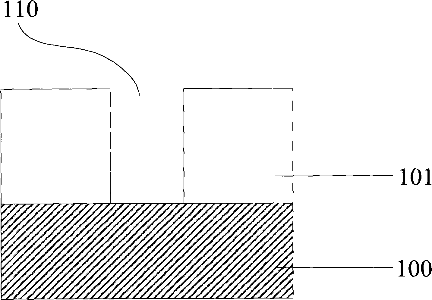
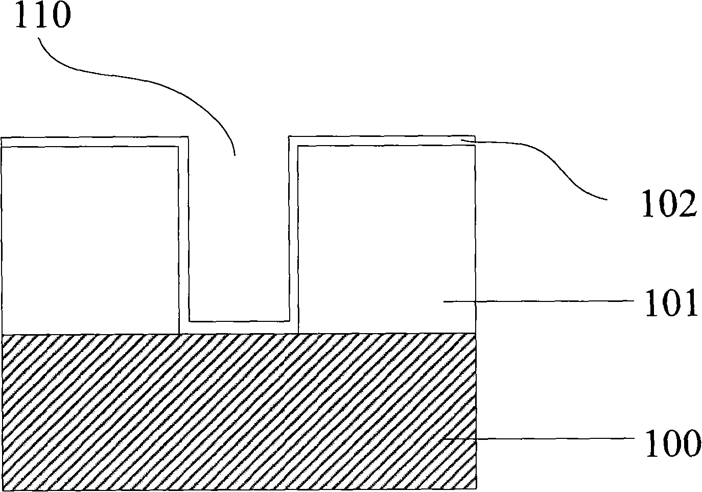
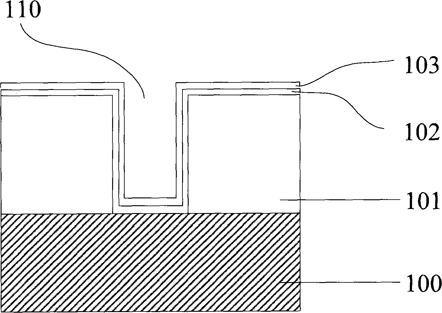
[0034] The invention provides a method for manufacturing a tungsten plug, which improves the formation process of the barrier layer. First, the adhesion layer is formed, and then the adhesion layer is nitrided, so that part of the adhesion layer forms a barrier layer, preventing the formation of the barrier layer due to deposition. Too many layers lead to the formation of "bumps" at the corners on both sides of the contact hole opening, thereby eliminating or reducing the internal voids formed during the manufacturing process of the tungsten plug, preventing the polishing liquid from immersing and corroding the tungsten plug during the chemical mechanical polishing process, and improving the performance. Product reliability.
[0035] In order to make the methods, features and advantages of the present invention more comprehensible, the specific implementation manners of the present invention will be described in detail below in conjunction with the accompanying drawings.
[00...
PUM
| Property | Measurement | Unit |
|---|---|---|
| Thickness | aaaaa | aaaaa |
| Thickness | aaaaa | aaaaa |
Abstract
Description
Claims
Application Information