

Annular light source test platform
A platform and light source technology, applied in the field of electromechanical, can solve problems such as damage to the reticle, and achieve the effect of improving the quality and improving the quality of the reticle.
- Summary
- Abstract
- Description
- Claims
- Application Information
AI Technical Summary
Problems solved by technology
Method used
Image

Examples
Embodiment Construction
[0024] In order to achieve the above-mentioned purpose and effect, the technical means and structure adopted by the present invention, the features and functions of the preferred embodiments of the present invention will be described in detail as follows in order to facilitate a complete understanding.
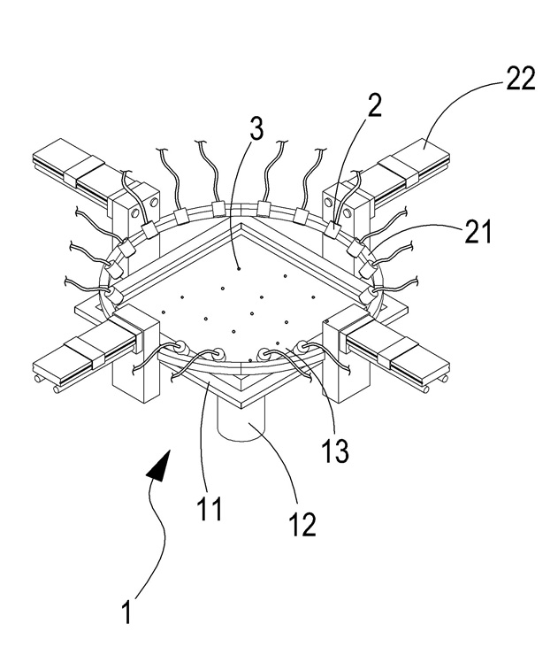
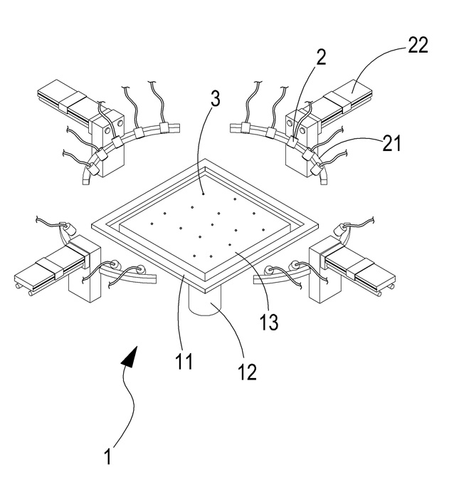
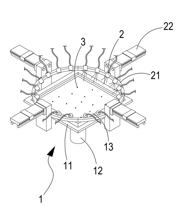
[0025] as attached figure 1 with attached figure 2 As shown, it is a perspective view and a three-dimensional exploded view of a preferred embodiment of the present invention, and it can be clearly seen that the present invention includes:
[0026] The supporting frame 1, the supporting frame 1 includes a supporting platform 11 for fixedly placing a preset photomask 13 and a support 12 supporting the supporting platform 11, the supporting frame 12 can freely rotate or move the supporting platform up and down. Set platform 11, between this bearing platform 11 and this support 12 is provided with an adjusting member that can make this bearing platform 11 rotate freely and can ...
PUM
 Abstract
Description
Claims
Application Information