Process for manufacturing whole gold-plated board
A production process and gold-plated area technology, which is applied to the production process of full-plate gold-plated plates, can solve the problems of gold-plated area collapse, poor gold-plated quality, and unclean etching, and achieve the effect of reduced total cost, low cost, and flexible production arrangement.
- Summary
- Abstract
- Description
- Claims
- Application Information
AI Technical Summary
Problems solved by technology
Method used
Image

Examples
Embodiment Construction
[0033] In order to describe the technical content, structural features, achieved goals and effects of the present invention in detail, the following will be described in detail in conjunction with the embodiments and accompanying drawings.
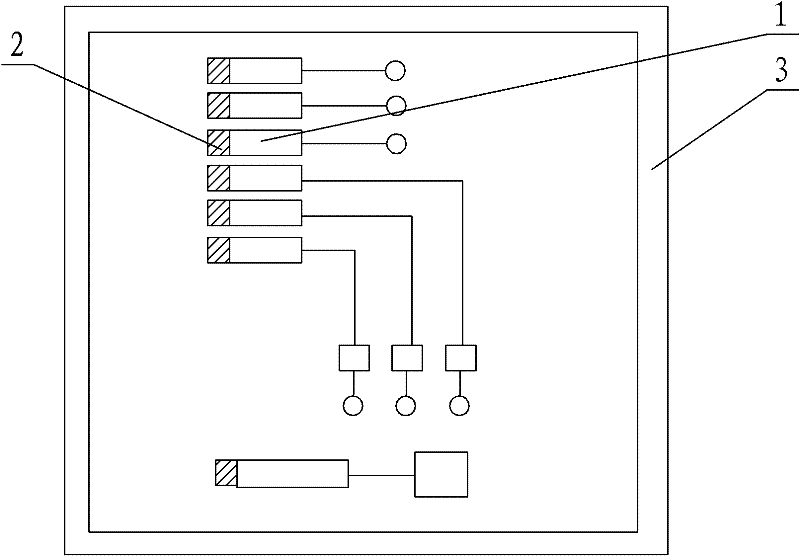
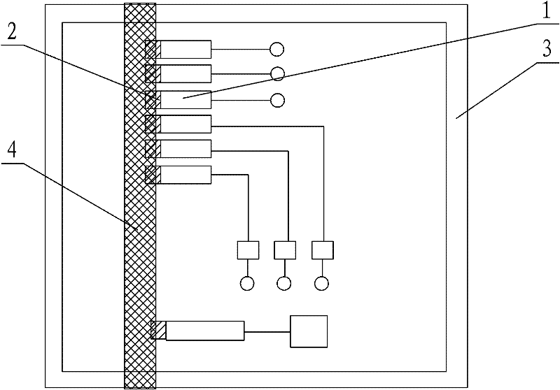
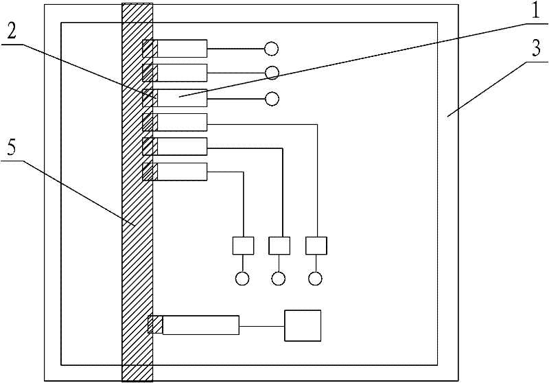
[0034] see Figure 1 to Figure 7 , as an embodiment of the manufacturing process of the full plate gold-plated plate of the present invention, comprises the following steps:
[0035] a. On the circuit board, make all in-board graphics and conductive auxiliary sides 3 with gold-plated area 1 and gold-plated auxiliary area 2 at one time, and the conductive auxiliary side 3 is not connected with the in-board graphics in this step, so The gold-plated auxiliary area 2 is electrically connected to the gold-plated area 1, such as figure 1 shown;
[0036] b. screen printing conductive ink 4 on the gold-plated auxiliary area 2, the conductive ink 4 covers all gold-plated auxiliary areas 2, and electrically connects between all gold-plated areas 1...
PUM
 Abstract
Description
Claims
Application Information
 - R&D Engineer
- R&D Manager
- IP Professional
- Industry Leading Data Capabilities
- Powerful AI technology
- Patent DNA Extraction
Browse by: Latest US Patents, China's latest patents, Technical Efficacy Thesaurus, Application Domain, Technology Topic.
© 2024 PatSnap. All rights reserved.Legal|Privacy policy|Modern Slavery Act Transparency Statement|Sitemap