

Manufacturing process of whole gold-plated panel
A technology of manufacturing process and gold-plated area, which is applied in the field of manufacturing process of full-plate gold-plated plate, and can solve problems such as gold-plated penetration, poor quality of gold-plated, and collapse of gold-plated area
- Summary
- Abstract
- Description
- Claims
- Application Information
AI Technical Summary
Problems solved by technology
Method used
Image

Examples
Embodiment Construction
[0032] In order to describe the technical content, structural features, achieved goals and effects of the present invention in detail, the following will be described in detail in conjunction with the embodiments and accompanying drawings.
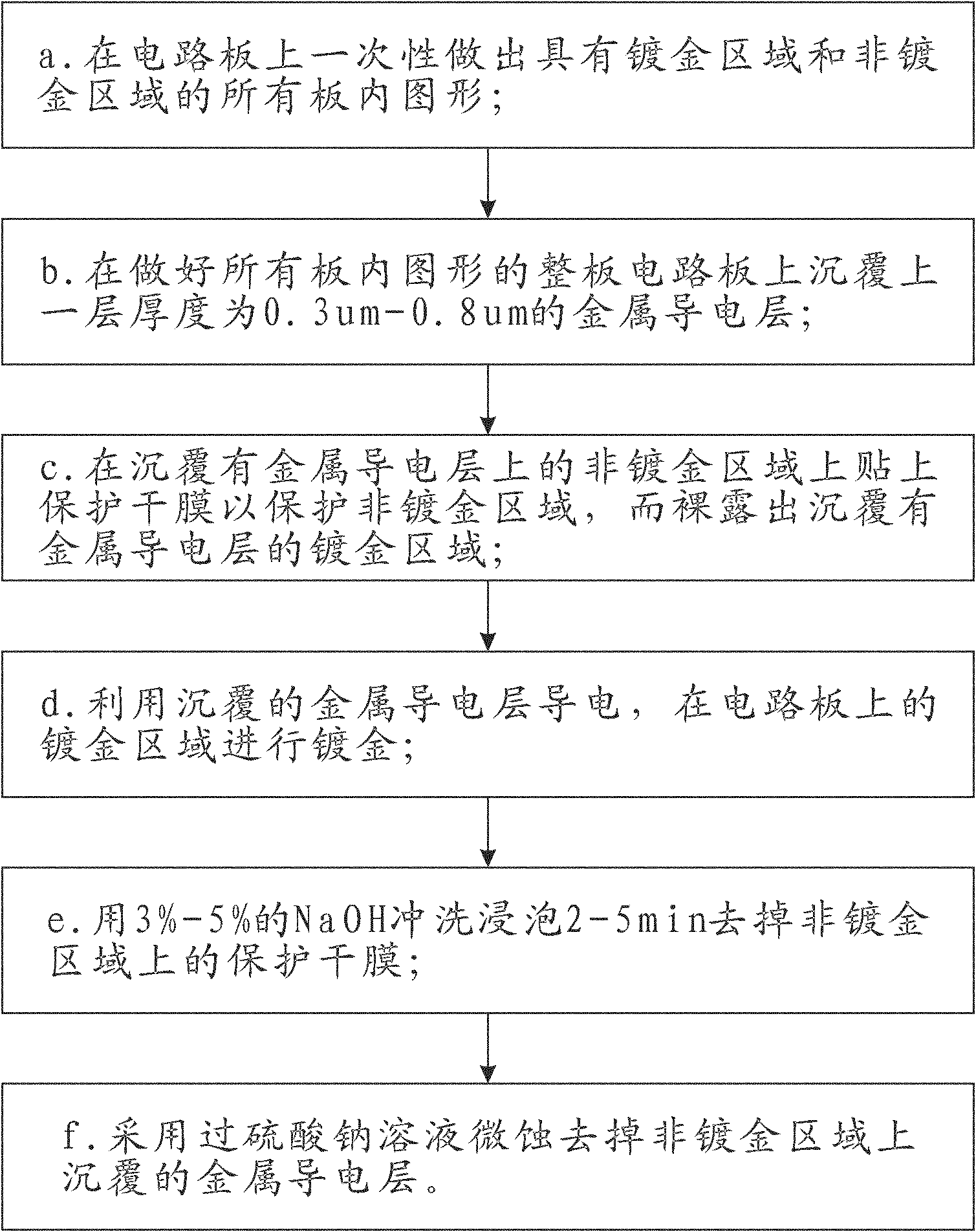
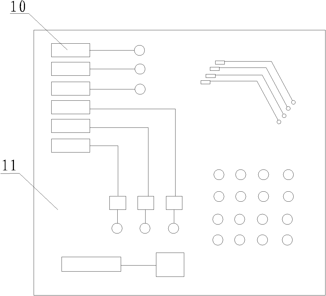
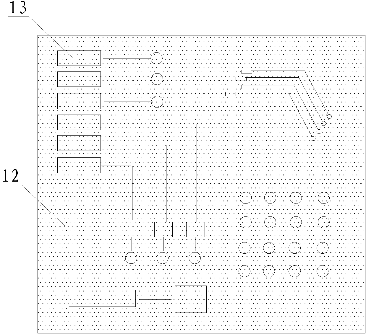
[0033] see Figure 1 to Figure 7 , the manufacturing process of full plate gold-plated plate of the present invention, comprises the following steps:
[0034] a. Make all in-board graphics with gold-plated area 10 and non-gold-plated area 11 on the circuit board at one time;
[0035] b. On the entire circuit board with all the graphics in the board, a metal conductive layer with a thickness of 0.3um to 0.8um is deposited; at this time, the gold-plated area becomes a metal conductive layer 13 covering the metal conductive layer, The non-gold-plated area 11 becomes the metal conductive layer 12 covering the upper metal conductive layer;
[0036] c. Paste a protective dry film on the non-gold-plated area covered with a metal conductive laye...
PUM
| Property | Measurement | Unit |
|---|---|---|
| Thickness | aaaaa | aaaaa |
Abstract
Description
Claims
Application Information