TFT-LCK array substrate and method for manufacturing same and method for repairing broken lines

A technology of array substrates and gate lines, which is applied in the field of TFT-LCD array substrates and its manufacturing and disconnection repair, and can solve the problems of different common voltages, etc.

Inactive Publication Date: 2011-04-20
BOE TECH GRP CO LTD +1
View PDF0 Cites 52 Cited by
  • Summary
  • Abstract
  • Description
  • Claims
  • Application Information

AI Technical Summary

Problems solved by technology

[0004] The first purpose of the present invention is to provide a TFT-LCD array substrate and its manufacturing method, which can effectively solve the technical defect of different common voltages at different positions on the common electrode line of the existing structure, and improve the display quality

Method used


Image

  • TFT-LCK array substrate and method for manufacturing same and method for repairing broken lines
  • TFT-LCK array substrate and method for manufacturing same and method for repairing broken lines
  • TFT-LCK array substrate and method for manufacturing same and method for repairing broken lines

Examples


Embodiment Construction

[0063] The technical solutions of the present invention will be described in further detail below with reference to the accompanying drawings and embodiments.

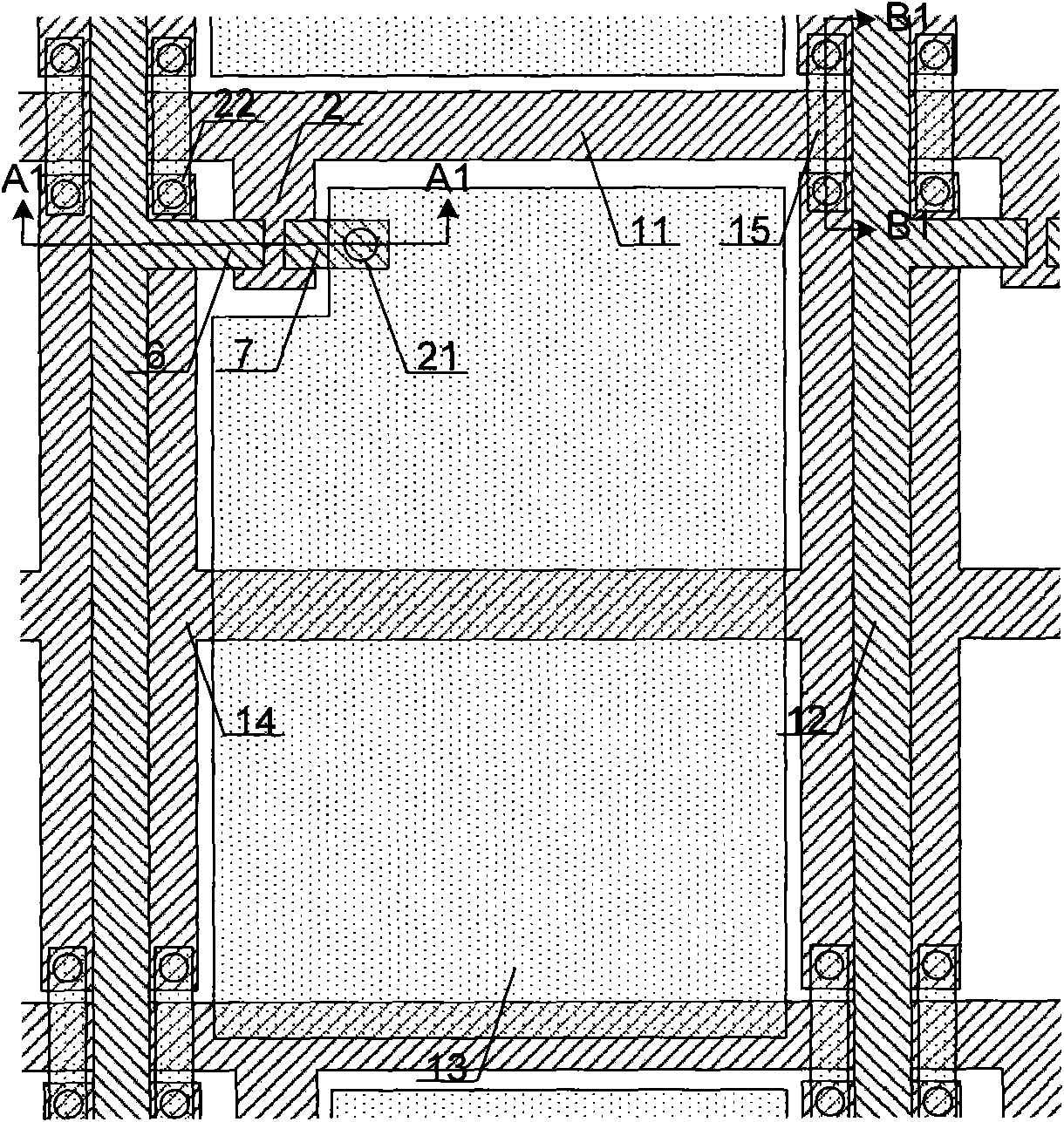
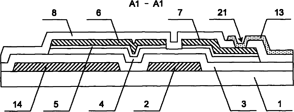
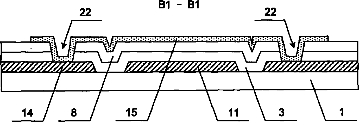
[0064] figure 1 It is a plan view of the first embodiment of the TFT-LCD array substrate of the present invention, reflecting the structure of a pixel unit, figure 2 for figure 1 The cross-sectional view of A1-A1 in the middle, image 3 for figure 1 Sectional view of B1-B1 direction in the middle. Such as Figure 1 ~ Figure 3 As shown, the main structure of the TFT-LCD array substrate in this embodiment includes gate lines 11, data lines 12, pixel electrodes 13, common electrode lines 14 and thin film transistors formed on the substrate 1, and gate lines 11 and data lines perpendicular to each other 12 defines the pixel area, the thin film transistor and the pixel electrode 13 are formed in the pixel area, the gate line 11 is used to provide an on or off signal to the thin film transistor, the data line 12 is use...


PUM


Abstract

The invention relates to a TFT-LCD array substrate and a method for manufacturing the same and a method for repairing broken lines. The TFT-LCD array substrate comprises grid lines, statistical lines, common electrode lines, pixel electrodes and thin film transistors. The common electrode lines have a matrix structure with interconnected horizontal electrode lines and vertical electrode lines. The horizontal electrode lines and the vertical electrode lines are arranged at the same layer as the grid lines. The horizontal lines have an integral structure while the vertical electrode lines have a disconnected structure located below the statistical lines and are linked with at least one connecting line to form an integral unit. The present invention, by the common electrode lines which form the matrix structure on the substrate, guarantees the same common voltage of each position of the common electrode lines and the accuracy of liquid crystal deflection, and enhances display quality. The method for repairing broken lines of the invention realizes grid line repair or statistical line repair through the matrix-shaped common electrode lines. In this way, repair is made less difficultlyand more conveniently with higher success rate, and poor performance caused by broken grid lines or broken statistical lines is effectively avoided.

Description

technical field [0001] The invention relates to a thin film transistor liquid crystal display and its manufacturing and maintenance method, in particular to a TFT-LCD array substrate and its manufacturing and disconnection repairing method. Background technique [0002] Thin Film Transistor Liquid Crystal Display (TFT-LCD for short) has the characteristics of small size, low power consumption, and no radiation. It has developed rapidly in recent years and occupies a dominant position in the current flat panel display market. The main structure of the TFT-LCD includes a TFT-LCD array substrate and a color filter substrate that are boxed together and the liquid crystal is sandwiched between them. The TFT-LCD array substrate is formed with gate lines, data lines, common electrode lines and arranged in a matrix. The thin film transistors and pixel electrodes of the color filter substrate are formed with a black matrix, color resin and common electrodes. By controlling the voltag...

Claims


Application Information

Patent Timeline
Patent Type & Authority Applications(China)
IPC IPC(8): G02F1/1362G02F1/1368H01L27/02H01L21/82H01L21/768G03F7/00
Inventor 张弥
Owner BOE TECH GRP CO LTD
Why Eureka
Try Eureka