
Method for manufacturing GaAs-based metal oxide semiconductor (MOS) device

A technology of MOS devices and substrates, applied in semiconductor/solid-state device manufacturing, electrical components, circuits, etc., can solve the problems that hinder the application of compound semiconductor MOSFETs, cannot obtain high-quality interface electrical properties, Fermi pinning, etc., and achieve Improve the interface quality, improve the electrical performance, the effect of small capacitance hysteresis

Inactive Publication Date: 2011-04-20
NANJING UNIV
View PDF5 Cites 6 Cited by
  • Summary
  • Abstract
  • Description
  • Claims
  • Application Information

AI Technical Summary

Benefits of technology

This patented technology allows for better control over how well an epilayered semiconductor device works when exposed to oxygen during manufacturing processes. Using specific techniques like chemical vapor deposition or atomic layer growth methods, we have discovered that adding certain elements into gallium nitride layers improves their electronic structure compared with pure germanium dioxides without these added materials. Additionally, controlling the composition ratio helps reduce impurities such as arsenic which may be introduced during production process. Overall, our technical effect is increased efficiency and reliability in producing advanced IIIA/V compound transistors used in modern electronics applications.

Problems solved by technology

This patented technical problem addressed by this patents relates to improving the performance of certain types of electronic components like Fin Field Effect Transistor (FinFet). These improvements require better understanding of how these structures work together during their operation due to factors including reduced energy usage caused by smaller sizes and improved manufacturing processes associated therewith. Current methods involve depositing layers called gate insulation films onto crystal surfaces or directly adding interlayer passivating agents into source gases containing gallium nitride.

Method used


Image

  • Method for manufacturing GaAs-based metal oxide semiconductor (MOS) device
  • Method for manufacturing GaAs-based metal oxide semiconductor (MOS) device
  • Method for manufacturing GaAs-based metal oxide semiconductor (MOS) device

Examples


Embodiment 1

[0022] 1) Substrate cleaning: The GaAs substrate was ultrasonically cleaned with acetone, ethanol, and isopropanol for 5 minutes in sequence, and then soaked in HCl aqueous solution with a volume ratio of 1:10 for 3 minutes.

[0023] 2) Substrate passivation: Clean the GaAs substrate with 8% volume ratio (NH 4 ) 2 Soak in S aqueous solution for 30 minutes;

[0024] 3) MOCVD deposits a thin layer of Gd 2 o 3 Control layer process: put the passivated GaAs substrate into the MOCVD reaction chamber immediately, deposit Gd 2 o 3 Thin layer, the thickness of the thin layer is 2nm, the deposition temperature is 500 °C, and the metal source used is tetramethylheptadione gadolinium: Gd(DPM) 3 [DPM=tris(2,2,6,6-tetramethyl-3-5-heptanedionato)];

[0025] 4) ALD deposition of ZrO 2 Gate dielectric layer process: Put the processed GaAs substrate into the ALD reaction chamber, and set the ALD deposition parameters as:

[0026] Reaction chamber temperature: 300 °C;

[0027] Reaction...

Embodiment 2

[0036] 1) Substrate cleaning: The GaAs substrate was ultrasonically cleaned with acetone, ethanol, and isopropanol for 3 minutes, and then soaked in HCl aqueous solution with a volume ratio of 1:10 for 4 minutes.

[0037] 2) Substrate passivation: Clean the GaAs substrate with 40% volume ratio (NH 4 ) 2 Soak in S aqueous solution for 30 minutes;

[0038] 3) MOCVD deposits a thin layer of Gd 2 o 3 Control layer process: put the passivated GaAs substrate into the MOCVD reaction chamber immediately, deposit Gd 2 o 3 Thin layer, the thickness of the thin layer is 1nm, the deposition temperature is 500 °C, and the metal source used is tetramethylheptadione gadolinium: Gd(DPM) 3 [DPM=tris(2,2,6,6-tetramethyl-3-5-heptanedionato)];

[0039] 4) ALD deposition Zr-Al-O gate dielectric layer process: put the processed GaAs substrate into the ALD reaction chamber, and set the ALD deposition parameters as follows:

[0040] Reaction chamber temperature: 250 °C;

[0041] Reaction so...

Embodiment 3

[0045] 1) Substrate cleaning: The GaAs substrate was ultrasonically cleaned with acetone, ethanol, and isopropanol for 10 minutes in sequence, and then soaked in HCl aqueous solution with a volume ratio of 1:10 for 5 minutes.

[0046] 2) Substrate passivation: Clean the GaAs substrate with 20% volume ratio (NH 4 ) 2 Soak in S aqueous solution for 40 minutes;

[0047] 3) MOCVD deposits a thin layer of Gd 2 o 3 Control layer process: put the passivated GaAs substrate into the MOCVD reaction chamber immediately, deposit Gd 2 o 3 Thin layer, the thickness of the thin layer is 3nm, the deposition temperature is 500 °C, and the metal source used is tetramethylheptadione gadolinium: Gd(DPM) 3 [DPM=tris(2,2,6,6-tetramethyl-3-5-heptanedionato)];

[0048] 4) ALD deposition of HfO 2 Gate dielectric layer process: Put the processed GaAs substrate into the ALD reaction chamber, and set the ALD deposition parameters as:

[0049] Reaction chamber temperature: 350 °C;

[0050] Reac...


PUM


Abstract

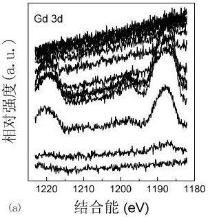
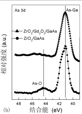
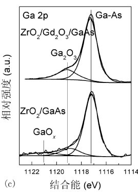
The invention discloses a method for manufacturing a GaAs-based metal oxide semiconductor (MOS) device, which comprises the following steps of: first washing a substrate, and impregnating the substrate with 8 to 40 volume percent of aqueous solution of (NH4)2S for 10 to 40 minutes for passivation; then depositing a thin Gd2O3 control layer by using metal organic chemical vapor deposition (MOCVD); and finally depositing a high-k gate dielectric layer by using atomic layer deposition (ALD). In the method, the thin Gd2O3 control layer is introduced so as to effectively suppress the formation of As oxides and Ga oxides at an interface, improve interface quality between gate dielectric and the GaAs substrate, effectively adjust energy band compensation between n-GaAs and a gate dielectric thin film and improve the electrical properties of the gate dielectric thin film. The GaAs-based MOS device exhibits relatively higher accumulated capacitance, relatively lower capacitive hysteresis and relatively lower leakage current density. The method is simple and has vast application prospect in the preparation of the GaAs-based metal oxide semiconductor field effect transistor (MOSFET) device.

Description


Claims


Application Information

Patent Timeline
Owner NANJING UNIV
Learn More