
Laser processing method of workpiece

A laser processing method and a technology for processed objects, which can be applied to laser welding equipment, metal processing equipment, manufacturing tools, etc., and can solve problems such as deviation from the predetermined dividing line

Active Publication Date: 2014-10-15
DISCO CORP
View PDF6 Cites 0 Cited by
  • Summary
  • Abstract
  • Description
  • Claims
  • Application Information

AI Technical Summary

Problems solved by technology

[0008] However, in the technology of the above-mentioned Patent Document 2, since the modified region along the first planned dividing line and the second planned dividing line arranged on the surface of the workpiece is formed in the central part in the thickness direction inside the workpiece, There are cases in which fractures generated starting from these modified regions at the time of division occur obliquely, thereby deviating from the planned division line.

Method used


Image

  • Laser processing method of workpiece
  • Laser processing method of workpiece
  • Laser processing method of workpiece

Examples


Embodiment approach 1

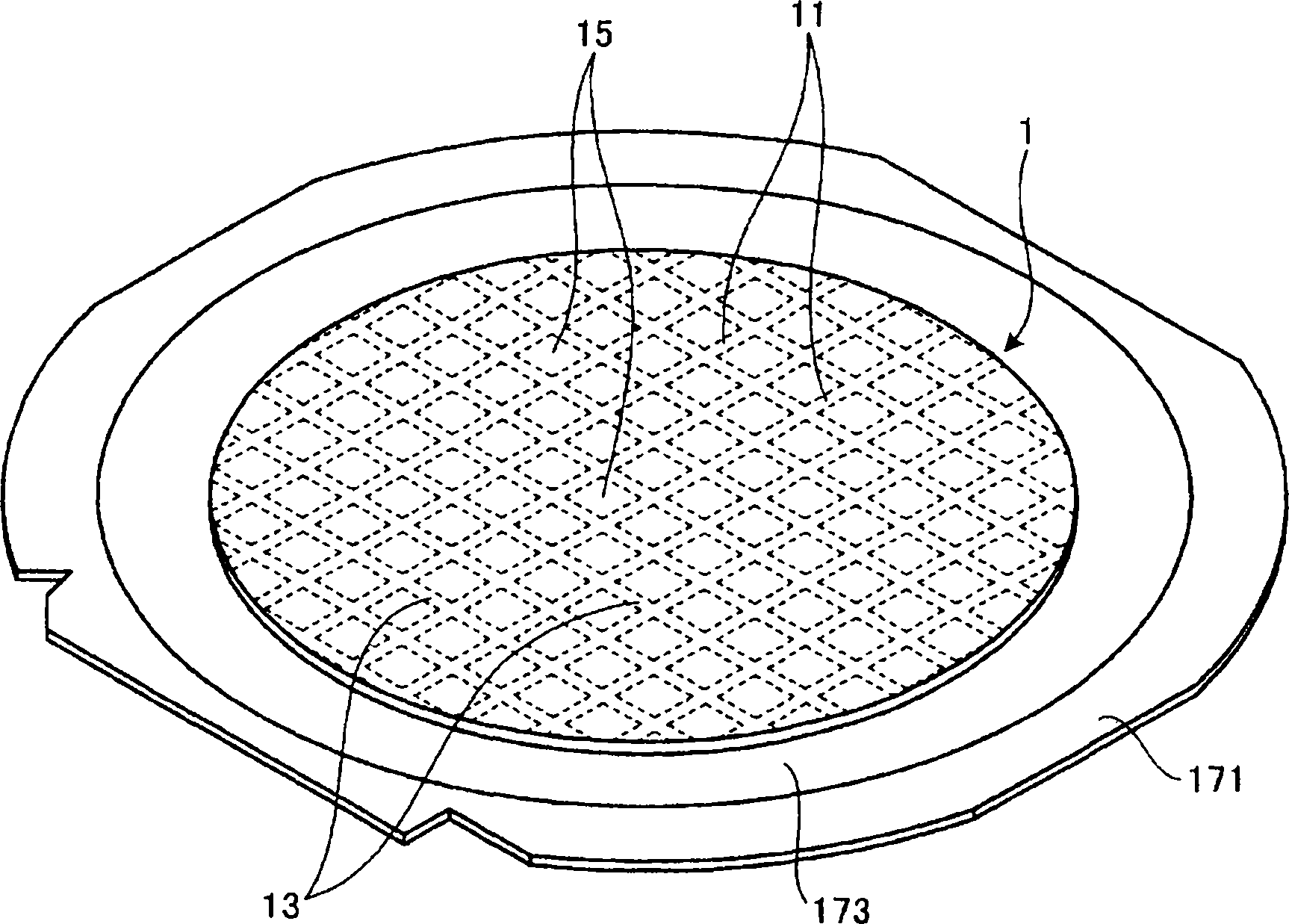
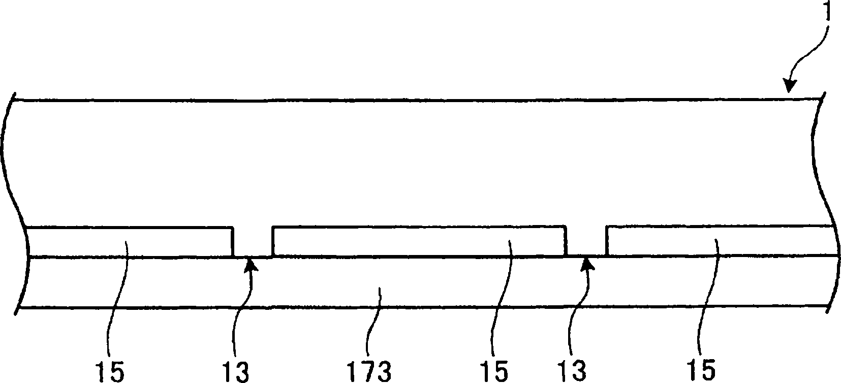
[0044] First, the workpiece to be processed in the processing method of Embodiment 1 will be described. figure 1 It is a perspective view showing a structural example of the workpiece 1 in the first embodiment. also, figure 2 It is a sectional view showing the inside of the workpiece 1 in the first embodiment. Such as figure 1 As shown, the workpiece 1 is configured to have a disc shape, and the first planned dividing line 11 and the second planned dividing line 13 are arranged in a grid on the surface side thereof, and the first planned dividing line 11 and the second planned dividing line 13 Functional elements 15 are formed in a plurality of rectangular areas divided by the second planned dividing line 13 . In addition, in the processing method of Embodiment 1, such as figure 1 with figure 2As shown, the workpiece 1 in the state supported by the ring frame 171 via the protective belt 173 made of a stretchable synthetic resin sheet is processed. More specifically, th...

Embodiment approach 2

[0081] In the first embodiment described above, when processing is performed by the processing device 2, the workpiece 1 is held with the back side exposed by the holding member 21, and the pulsed laser beam is irradiated from the rear side of the workpiece 1 to form the first laser beam. Modified area and second modified area. On the other hand, in Embodiment 2, the workpiece 1a is held with the surface side exposed by the holding member 21, and pulsed laser light is irradiated from the surface side of the workpiece 1a. The surface on the side irradiated with pulsed laser beams is not particularly limited, as long as it is formed sequentially from the modified region formed at a position farther from the surface on the side irradiated with pulsed laser beams in the thickness direction. Hereinafter, Embodiment 2 will be described in detail.

[0082] Figure 13 It is a perspective view showing a structural example of a workpiece 1a according to the second embodiment. also, ...

Embodiment approach 3

[0113] Figure 20 It is a perspective view explaining the structure of the semiconductor device 5b in Embodiment 3. Such as Figure 20 As shown, the semiconductor device 5 b in Embodiment 3 is configured by mounting a chip 10 b on a glass substrate 51 via an adhesive resin layer 53 . The chip 10 b is obtained by implementing the processing method described in the first embodiment or the second embodiment, and the chip 10 b is equivalent to the chip 10 in the first embodiment or the chip 10 a in the second embodiment. In addition, the adhesive resin layer 53 is, for example, an epoxy-based anisotropic conductive film (ACF: Anisotropic Conductive Film), which electrically and physically connects the glass substrate 51 and the chip 10 b by thermocompression bonding.

[0114] In the method of manufacturing the semiconductor device 5 b , first, an anisotropic conductive adhesive film used as the adhesive resin layer 53 is disposed on the glass substrate 51 . Then, the chip 10b i...


PUM

PropertyMeasurementUnit
lengthaaaaaaaaaa
thicknessaaaaaaaaaa

Abstract

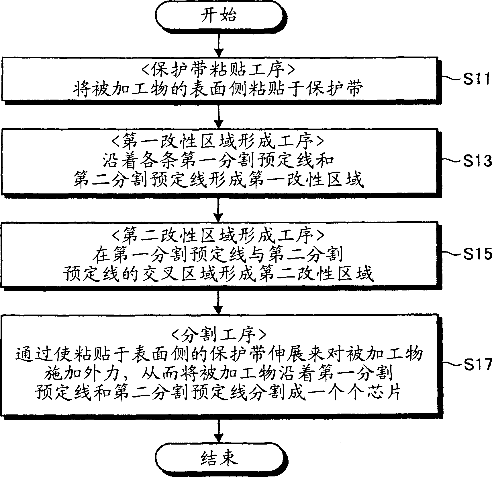
The present invention provides a laser processing method of a workpiece capable of dividing the workpiece with high precision along a planned dividing line. The processing method in a certain embodiment includes: a first modified region forming step of forming a first modified region (111) along a first planned dividing line and a second planned dividing line in the vicinity of the surface of the workpiece (1). ); the second modified region forming step, between the back surface of the workpiece (1) and the first modified region (111) formed inside the workpiece (1) in the first modified region forming step forming a second modified region (113) at a predetermined position and at the crossing region of the first planned dividing line and the second planned dividing line; (113) External force is applied to the workpiece (1), so that the workpiece (1) is divided into individual chips along the first planned dividing line and the second planned dividing line.

Description

technical field [0001] The present invention relates to a laser processing method for processing a workpiece (workpiece: workpiece) such as a semiconductor wafer. Background technique [0002] In the manufacturing process of a semiconductor device, first planned dividing lines and second planned dividing lines are arranged in a grid pattern on the surface of a plate-like workpiece such as a semiconductor wafer, Functional elements are formed in the area demarcated by the predetermined line. Then, individual chips are manufactured by dividing the workpiece on which the functional elements are formed along the first planned dividing line and the second planned dividing line. [0003] Here, as a method of dividing the workpiece along the first planned dividing line and the second planned dividing line, a laser processing method using a pulse-shaped laser beam for processing in an infrared region having transmittance to the workpiece has been tried. Laser beams (pulsed laser b...

Claims


Application Information

Patent Timeline
Patent Type & Authority Patents(China)
IPC IPC(8): H01L21/78B23K26/57H01L21/301
CPCB23K26/367B23K26/4075B23K26/40B23K26/364B23K2103/50
Inventor 植木笃
Owner DISCO CORP
Learn More