
Sonic wave resonator and processing method thereof

An acoustic wave resonator and passivation layer technology, applied in electrical components, impedance networks, etc., can solve the problems of poor SMRQ value, reduce the effective coupling coefficient of SMR, etc., to achieve relaxation requirements, reduce frequency offset, and weaken the effect of adsorption

Active Publication Date: 2011-04-20
ROFS MICROSYST TIANJIN CO LTD
View PDF2 Cites 29 Cited by
  • Summary
  • Abstract
  • Description
  • Claims
  • Application Information

AI Technical Summary

Problems solved by technology

The additional acoustic reflective layer will reduce the effective coupling coefficient of SMR, and will produce additional acoustic energy loss mechanism, which will cause the overall Q value of SMR to be worse than that of FBAR

Method used


Image

  • Sonic wave resonator and processing method thereof
  • Sonic wave resonator and processing method thereof
  • Sonic wave resonator and processing method thereof

Examples


Embodiment Construction

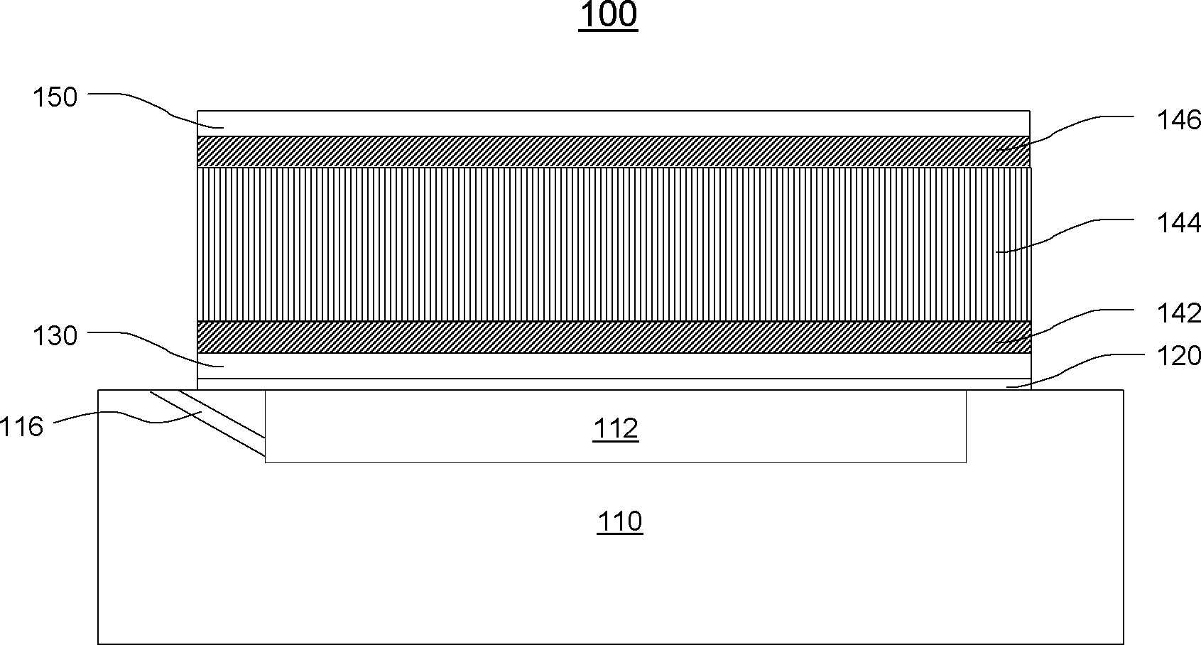
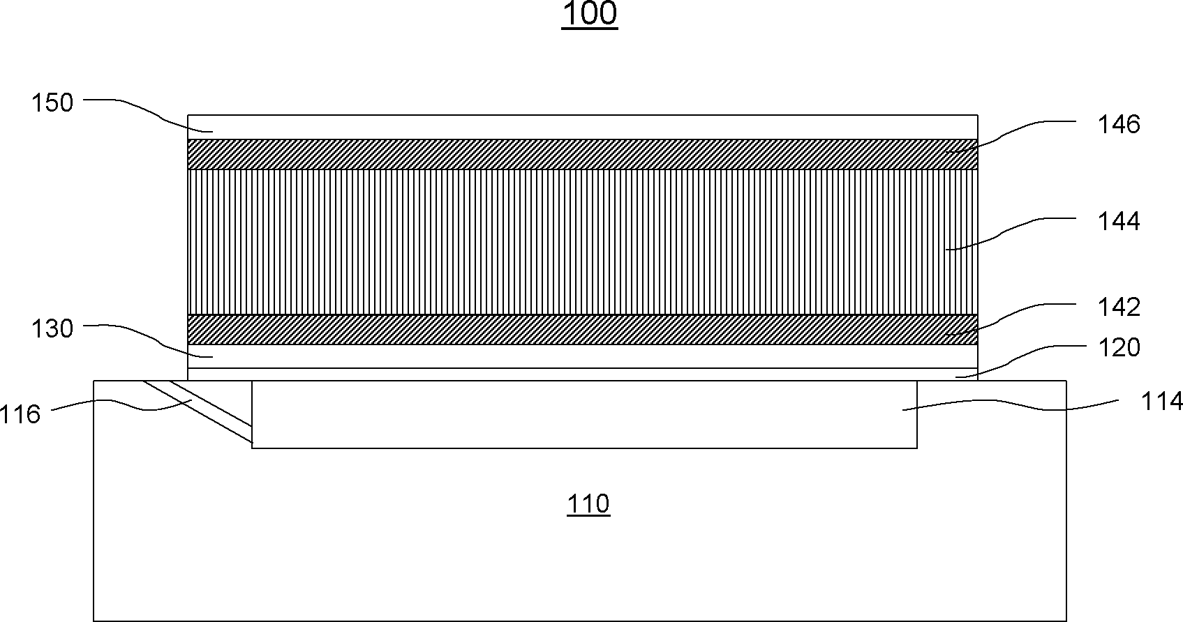
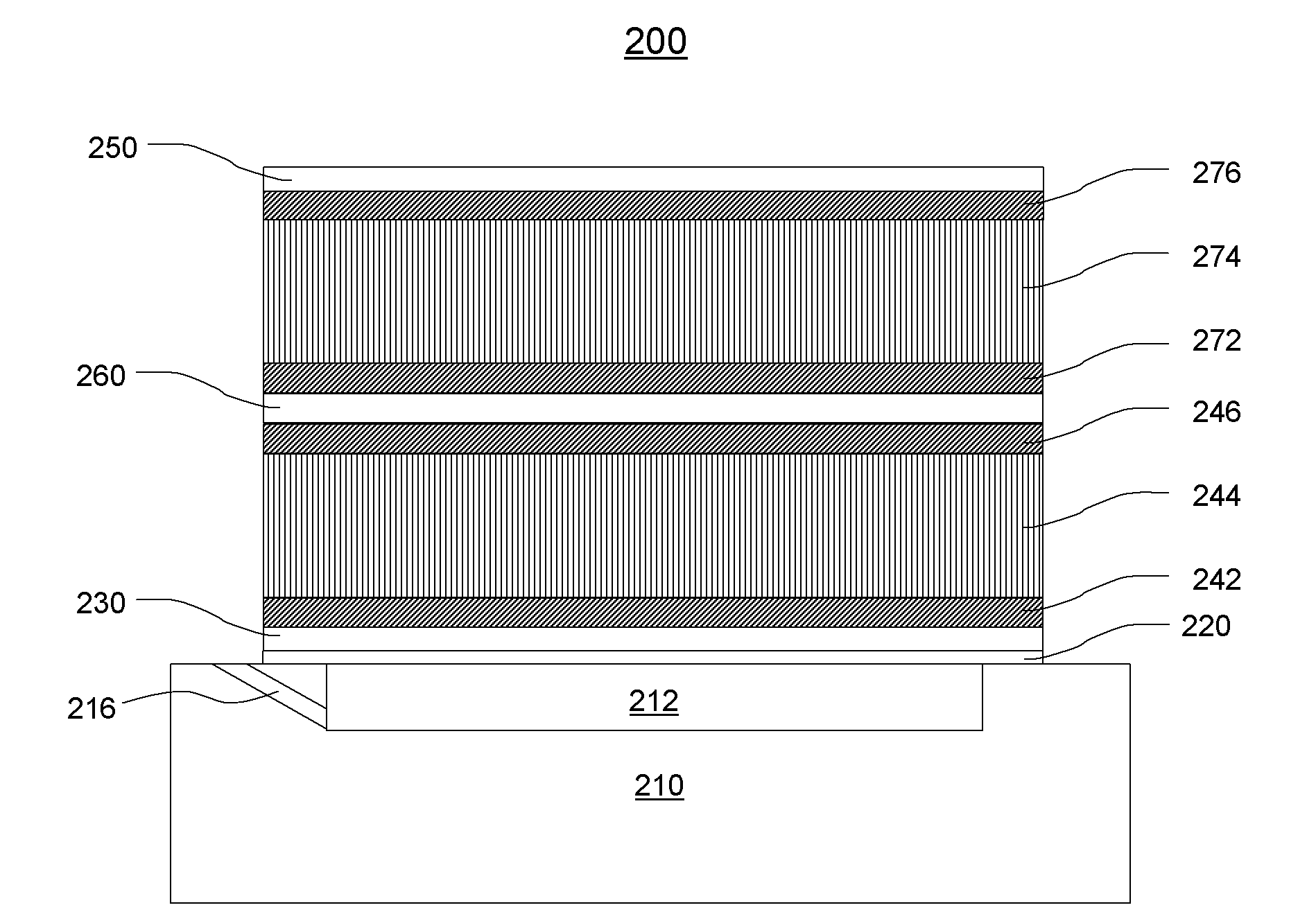
[0090] The acoustic wave resonator and its processing method of the present invention will be described in detail below with reference to the embodiments and the accompanying drawings.

[0091] The invention will be described in detail hereinafter with reference to the accompanying drawings, typical examples of which are also shown here. While the invention may be embodied in many different forms, the invention is not limited to the examples described herein. Rather, these examples are provided so that this technical description will be thorough and complete, and will fully convey the scope of the invention to those skilled in the art. The same reference numerals represent the same parts throughout.

[0092] An example of the invention is associated with a method of manufacturing an acoustic wave device. FBAR as an acoustic wave device will be described in the following examples.

[0093] Examples of the present invention are described with reference to the accompanying dra...


PUM

PropertyMeasurementUnit
Thicknessaaaaaaaaaa

Abstract

The invention discloses a sonic wave resonator and a processing method thereof. The sonic wave resonator comprises a substrate provided with an air cavity, a first passivation layer, a seeding layer, a multilayer structure, and a second passivation layer, wherein the first passivation layer is formed on the substrate and is above the air cavity, the seeding layer is formed on the first passivation layer which prevents the interaction between the seeding layer and the ambient environment of the resonator, the multilayer structure is formed on the seeding layer, and the second passivation layeris formed on the multilayer structure. The processing method comprises the steps of: providing the substrate with a sacrifice layer, forming the first passivation layer on the sacrifice layer and extending the first passivation layer to the whole substrate, forming the seeding layer on the first passivation layer, forming the multilayer structure on the seeding layer, forming the second passivation layer on the upper surface of the multilayer structure, and removing the sacrifice layer from the substrate to form the air cavity. The processing method can alleviate the adsorption of materials on the surface of the resonator, eliminate or alleviate the resonator frequency shift generated due to the influence of ambient air or a damp environment, lowers the requirements on the sealing packaging of the resonator to a great extent, and greatly reduces the manufacturing cost of the device.

Description

technical field [0001] The invention relates to an acoustic wave resonator. In particular, it relates to an acoustic wave resonator with one or more passivation layer structures and a processing method thereof. Background technique [0002] The simple structure of a thin-film bulk wave (BAW) resonator consists of opposing planar electrodes with a piezoelectric material sandwiched between them. Under operating conditions, applying a voltage across the electrodes results in a time-varying electric field within the piezoelectric layer. The electric field forms a bulk acoustic wave in the direction that causes the piezoelectric layer to vibrate, and then forms a resonance. The sound wave travels in the direction of the electric field and is reflected back off the edge of the electrode. Bulk wave (BAW) resonators are usually fabricated by sequentially depositing a bottom electrode, a piezoelectric layer, and a top electrode on the upper surface of a substrate. Therefore, the ...

Claims


Application Information

Patent Timeline
IPC IPC(8): H03H9/17H03H3/02
Inventor 庞慰张浩
Owner ROFS MICROSYST TIANJIN CO LTD
Learn More