
Key circuit board, keyboard and mobile phone

A circuit board and button technology, applied in circuits, telephone structures, printed circuit components, etc., can solve problems such as burning processing chips and system abnormalities, and achieve the effect of ensuring circuit safety and preventing electrostatic interference.

Active Publication Date: 2011-04-27
JUANCHENG RUIDING TECH CO LTD
View PDF4 Cites 2 Cited by
  • Summary
  • Abstract
  • Description
  • Claims
  • Application Information

AI Technical Summary

Problems solved by technology

[0003] Since the button is the most frequent contact between the electronic device and the human body, the button area is the most frequent area where the electronic device encounters the electrostatic discharge of the human body. In the existing technical solution, when the human body with static electricity touches the button, it may Static electricity will be released to the keys, which can easily cause system abnormalities or even burn the processing chip

Method used


Image

  • Key circuit board, keyboard and mobile phone
  • Key circuit board, keyboard and mobile phone
  • Key circuit board, keyboard and mobile phone

Examples


Embodiment Construction

[0013] Regarding the features and technical content of the present invention, please refer to the following detailed description and accompanying drawings, which are provided for reference and illustration only, and are not intended to limit the present invention.

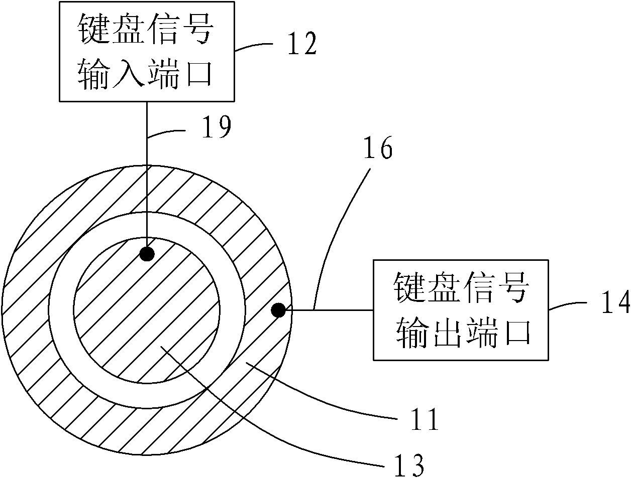
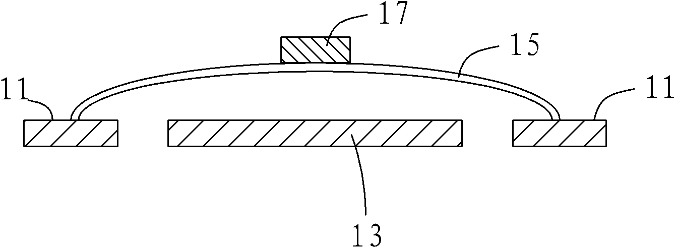
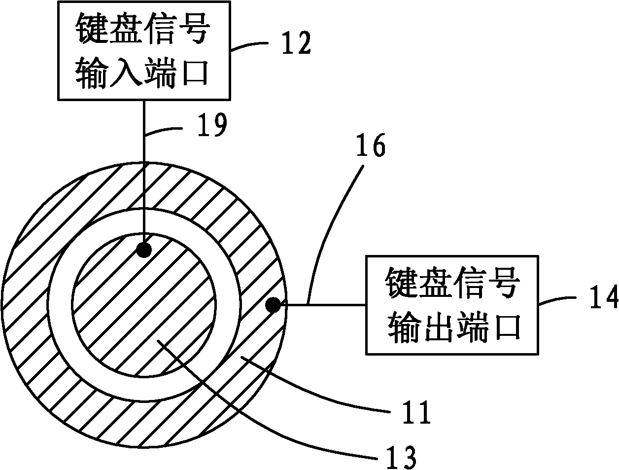
[0014] See figure 1 , figure 1 It is a schematic block diagram of the button circuit board according to the first embodiment of the present invention. Such as figure 1 As shown, the button circuit board of the present invention includes pads arranged on the button circuit board, and the pads include a central pad 13 and peripheral pads 11 arranged on the periphery of the central pad 13, and the central pad 13 passes through a first wire 19 It is electrically connected to the keyboard signal input port 12 of the processing chip (not shown), and the peripheral pad 11 is electrically connected to the keyboard signal output port 14 of the processing chip through the second wire 16 .

[0015] Among them, the input im...


PUM


Abstract

The invention provides a key circuit board. The key circuit board comprises bonding pads which are arranged on the key circuit board, wherein the bonding pads comprise a central bonding pad and a peripheral bonding pad which is arranged at the periphery of the central bonding pad; the central bonding pad is electrically connected to a keyboard signal input port of a processing chip through a first conducting wire; and the peripheral bonding pad is electrically connected to a keyboard signal output port of the processing chip through a second conducting wire. The invention also provides a keyboard and a mobile phone. In the mode, the technical scheme provided by the invention can effectively prevent electrostatic interference so as to guarantee circuit safety.

Description

【Technical field】 [0001] The invention relates to the technical field of printed circuit boards, in particular to a button circuit board, a keyboard and a mobile phone. 【Background technique】 [0002] With the development of electronic technology, electronic equipment often needs to use the human-computer interaction module to obtain user commands to perform corresponding actions. In the existing human-computer interaction module, the cost of pressing buttons is reasonable and the efficiency is better. Therefore, generally speaking, it will A human-computer interaction module that uses buttons as an electronic device. In the prior art, a printed circuit board (Printed Circuit Board, PCB for short) is often used to design the button circuit board. [0003] Since the button is the most frequent contact between the electronic device and the human body, the button area is the most frequent area where the electronic device encounters the electrostatic discharge of the human body...

Claims


Application Information

Patent Timeline
IPC IPC(8): H01H13/78H01H13/81H05K1/11H04M1/23
Inventor 苏海波
Owner JUANCHENG RUIDING TECH CO LTD
Learn More