Package for light emitting diode, light emitting device, and light emitting device manufacturing method

A technology for light-emitting diodes and light-emitting devices, which is applied in electrical components, electrical solid-state devices, circuits, etc., to achieve the effects of high reliability, long life, and excellent mass productivity.

Inactive Publication Date: 2011-04-27
CI KASEI COMPANY
View PDF2 Cites 7 Cited by
  • Summary
  • Abstract
  • Description
  • Claims
  • Application Information

AI Technical Summary

Problems solved by technology

In addition, there is a problem of strength in the bonding between the metal substrate and the insulating material.

Method used


Image

  • Package for light emitting diode, light emitting device, and light emitting device manufacturing method
  • Package for light emitting diode, light emitting device, and light emitting device manufacturing method
  • Package for light emitting diode, light emitting device, and light emitting device manufacturing method

Examples


Embodiment 1

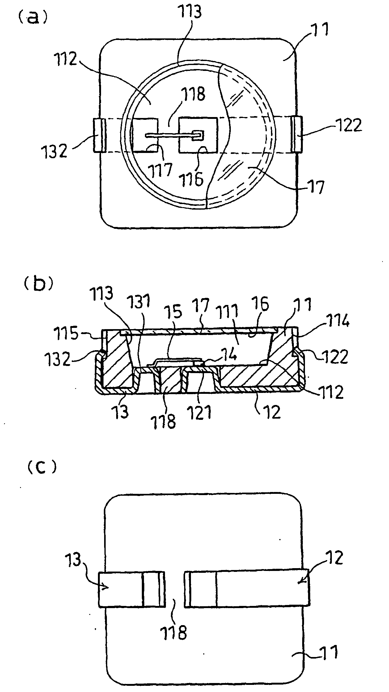
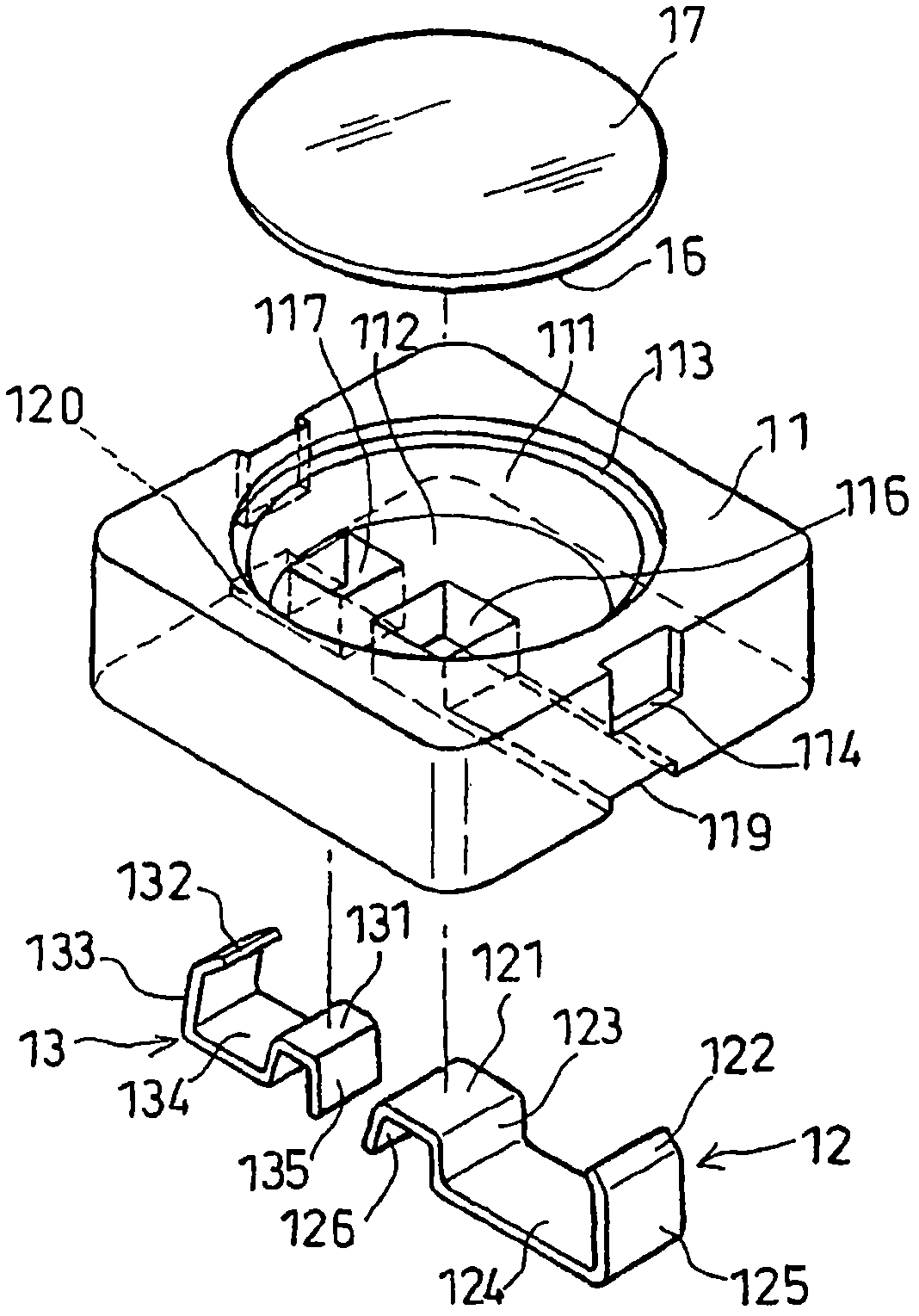
[0115] figure 1 (a) to (c) are the first embodiment of the present invention, (a) is a top view of the light emitting device, (b) is a cross-sectional view of the light emitting device, and (c) is a bottom view of the light emitting device. figure 2 It is an assembly perspective view for explaining the first embodiment of the light emitting diode package of the present invention. exist figure 1 (a)~(c) and figure 2 Among them, the package for a light emitting diode is constituted by at least a ceramic molded body 11 , a first conductive member 12 , and a second conductive member 13 .

[0116] The above-mentioned ceramic molded body 11 includes a space 111 composed of recesses, an inner bottom 112 as the bottom of the space, a reflective surface 113 formed around the inner bottom 112, a first opening 116 and a first opening 116 formed on the inner bottom 112. Two openings 117, the first engaging portion 114 and the second engaging portion 115 formed on the side, and the ...

Embodiment 2

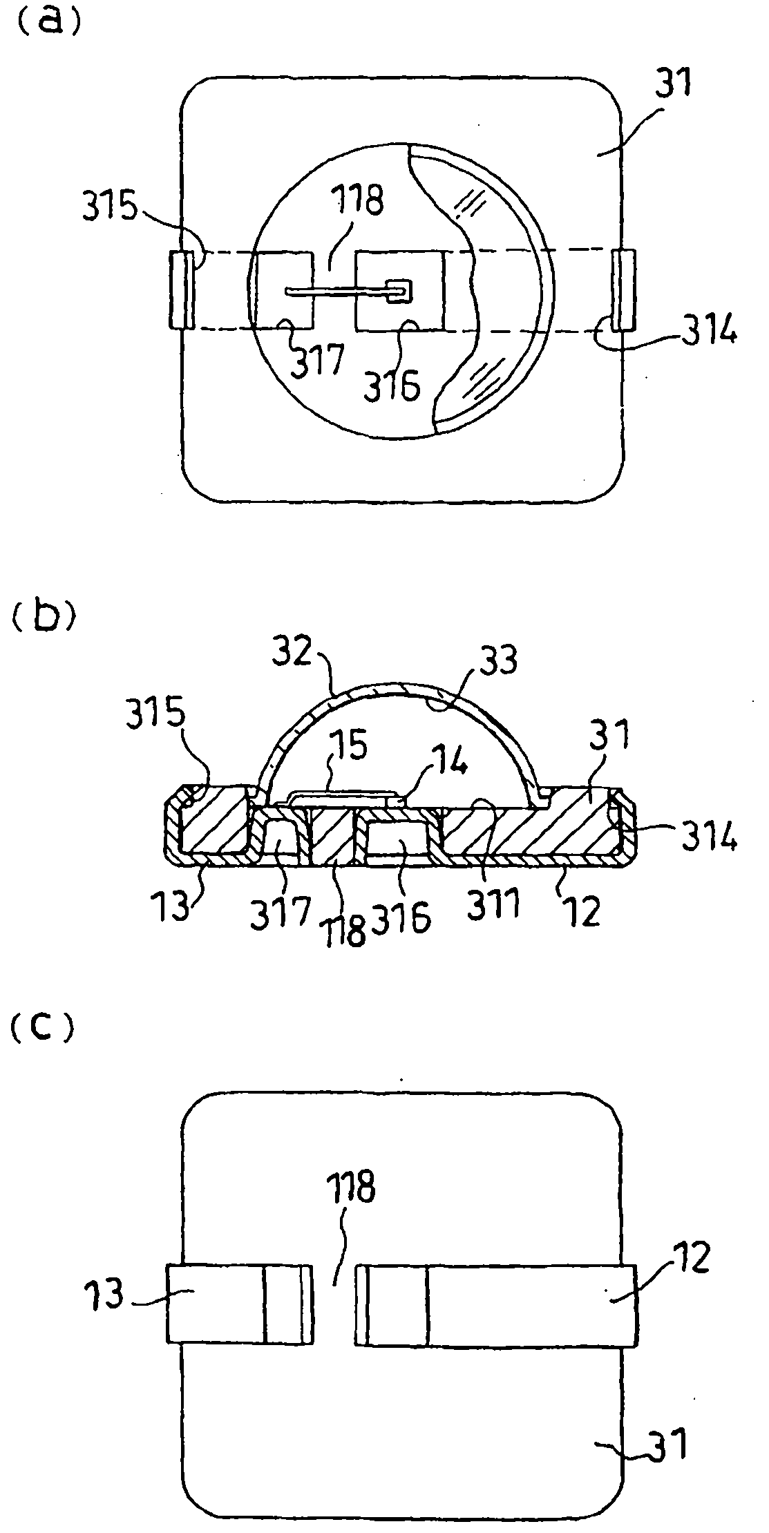
[0123] image 3 (a) to (c) are the second embodiment of the present invention, (a) is a top view of the light emitting device, (b) is a cross-sectional view of the light emitting device, and (c) is a bottom view of the light emitting device. exist image 3 In (a) to (c), the light-emitting device of the second embodiment is different from the first embodiment in that a ceramic substrate 31 and a hemispherical cover 32 on the ceramic substrate 31 are provided, and the cover 32 is formed with fluorescent light on the inner surface. The membrane body 33 of the body. A first opening 316 and a second opening 317 are formed on the ceramic substrate 31 , and a first engaging portion 314 and a second engaging portion 315 are formed on both sides.

[0124] The first conductive member 12 and the second conductive member 13 , the first opening 316 and the second opening 317 , the upper and lower electrode type LEDs 14 , and the metal member 15 are the same as those of the first embodim...

Embodiment 3

[0126] Figure 4 (a) and (b) are the third embodiment of the present invention, (a) is a plan view of a light emitting device in which a plurality of upper and lower electrode type light emitting diodes are connected in series, and (b) is a cross-sectional view of the light emitting device. exist Figure 4 In (a) and (b), in the light emitting device of the third embodiment, a plurality of light emitting devices of the second embodiment are connected in series on one ceramic substrate 41 . The first conductive member 12 and the fourth conductive member 13 of the third embodiment are the same as those of the second embodiment. The second conductive member 45 and the third conductive member 46 are provided with convex portions at both end portions, and are respectively fitted into the openings.

[0127] The upper and lower electrode type light emitting diodes 14-1, 14-2, 14-3 are placed on the convex portion of the above-mentioned conductive member, and are joined to the other...


PUM


Abstract

Provided are a light emitting diode package having a light emitting diode mounted thereon, a light emitting device having a vertical electrode type light emitting diode mounted on the light emitting diode package, and a manufacturing method for manufacturing the light emitting device. The light emitting diode package is configured to include at least a molding, and a first clip (122) and a second clip (123) fitted on the molding. The molding has at least a first opening (1212) and a second opening (1213) molded in the bottom portion. The molding also has a reflecting portion (1214) molded around the first opening (1212) and the second opening (1213) for reflecting a light. The molding further has a fluorescent film member mounting portion (1113) formed integrally for mounting an fluorescent film member (116) in the opening of the reflecting portion (1214). The first clip (122) has a light emitting diode mounting projection (1221) formed at the substantially central portion thereof for mounting the light emitting diode and made to engage elastically with the molding at both ends thereof. The first clip (122) is made to engage with the molding at both ends thereof. The second clip (123) has a jointing projection formed to engage elastically with the molding at both ends thereof.

Description

technical field [0001] The present invention relates to a package for a light emitting diode in which at least one light emitting diode is mounted, a light emitting device, and a method of manufacturing the light emitting device. The present invention relates to a package for a light-emitting diode, a light-emitting device, and a method of manufacturing the light-emitting device, which have a structure capable of supplying a large current to the above-mentioned light-emitting diode. [0002] The present invention relates to such a light-emitting diode package, a light-emitting device, and a method for manufacturing the light-emitting device. The light-emitting diode package is at least composed of a substrate integrally formed inside a reflective frame, an opening formed in the substrate, and an opening fitted in the opening. Part of the wire-shaped conductive member. [0003] The present invention relates to a light-emitting diode package, a light-emitting device, and a meth...

Claims


Application Information

Patent Timeline
Patent Type & Authority Applications(China)
IPC IPC(8): H01L33/00H01L33/48H01L33/62
CPCH01L2924/0002H01L33/486H01L33/62H01L2224/48247H01L2224/45144H01L2924/00014
Inventor 伏见宏司
Owner CI KASEI COMPANY
Why Eureka
Try Eureka