Method for measuring contact hole

A technology for contact hole and optical measurement, which is applied in the direction of measuring device, color/spectral characteristic measurement, semiconductor/solid-state device testing/measurement, etc. The contact hole is complicated and time-consuming, so as to achieve the effect of enriching parameters, solving the inability to measure the height and side wall angle of the contact hole, and improving efficiency

Inactive Publication Date: 2011-05-11
SEMICON MFG INT (SHANGHAI) CORP
View PDF0 Cites 15 Cited by
  • Summary
  • Abstract
  • Description
  • Claims
  • Application Information

AI Technical Summary

Problems solved by technology

[0021] As can be seen from the above, although the existing technology measures the parameters of the contact hole online, which has certain advantages compared to offline measurement, but when measuring the parameters of the contact hole in the prior art, different measurement tools are required, and When testing whether the contact hole is completely etched, it is necessary to perform CMP on the conductive metal in the contact hole before testing. Once it is found that it does not meet the target specification, the filled conductive metal can only be removed and etched again
Not only is the process of measuring contact holes more complicated and time-consuming, but also reduces the production efficiency of the entire integrated circuit
Moreover, the height and sidewall angle of the contact hole cannot be measured in the prior art, and the lack of these data makes it impossible to reflect the situation of the contact hole well

Method used


Image

  • Method for measuring contact hole
  • Method for measuring contact hole
  • Method for measuring contact hole

Examples


Embodiment Construction

[0044] In order to make the object, technical solution, and advantages of the present invention clearer, the present invention will be further described in detail below with reference to the accompanying drawings and examples.

[0045] The present invention has been described in detail using schematic diagrams. When describing the embodiments of the present invention in detail, for the convenience of explanation, the schematic diagram showing the structure will not be partially enlarged according to the general scale, which should not be used as a limitation of the present invention. In addition, in actual production In , the three-dimensional space dimensions of length, width and depth should be included.
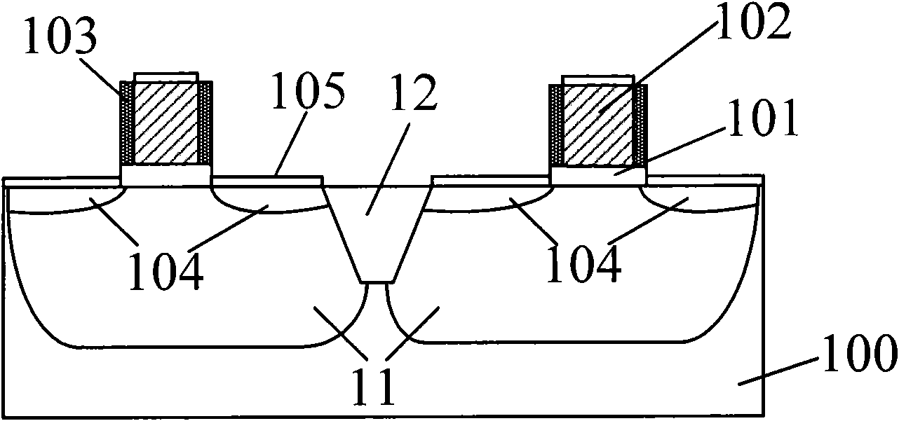
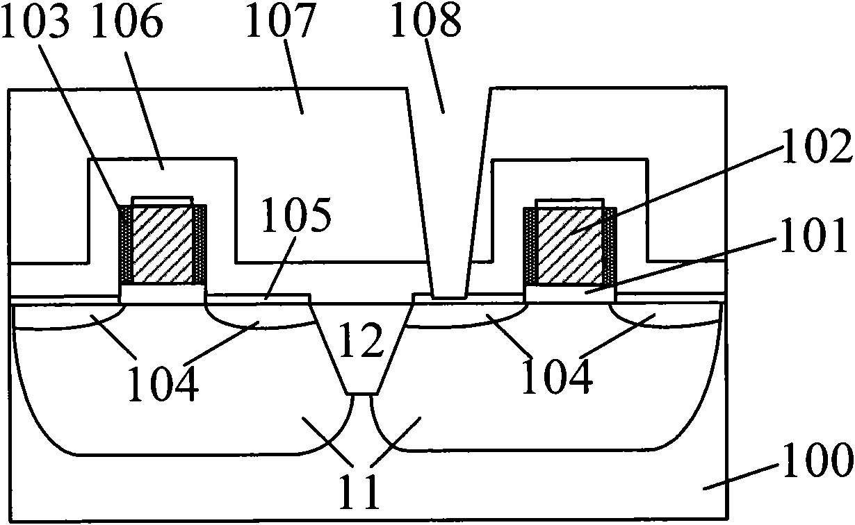
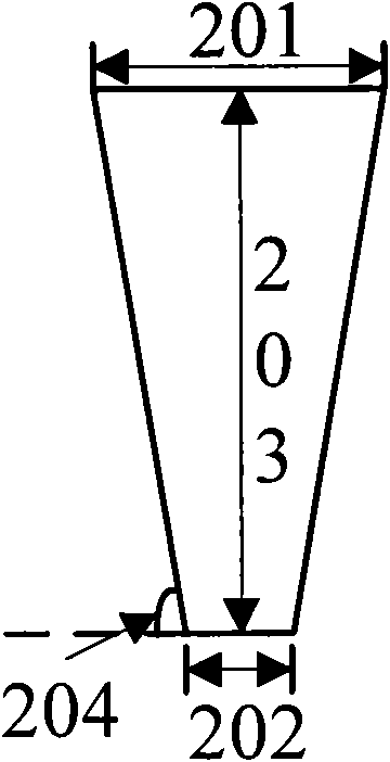
[0046] The core idea of ​​the present invention is: use the optical measurement method to measure the contact hole online, and the parameters to be measured include the upper characteristic size 201 of the contact hole, the bottom characteristic size 202 of the contact hole...


PUM


Abstract

The invention discloses a method for measuring a contact hole, and the measuring parameters of the contact hole comprise: an upper port characteristic dimension of the contact hole, a bottom characteristic dimension of the contact hole, the height of the contact hole, a side wall angle of the contact hole and whether etching of the contact hole is complete; in the method, after the contact hole is formed by etching, the contact hole is measured on line by adopting an optical measurement method, and simultaneously each parameter is obtained. The efficiency of measuring the contact hole is improved greatly by adopting the method for measuring the contact hole.

Description

technical field [0001] The invention relates to the technical field of semiconductor manufacturing, in particular to a method for measuring a contact hole. Background technique [0002] At present, when making a semiconductor integrated circuit, after the semiconductor device layer is formed, it is necessary to make a contact hole (contact) on the semiconductor device layer of the wafer. It plays an important role in the structure composition of semiconductor devices. [0003] Before introducing the etching of the contact hole, first briefly introduce the composition of the semiconductor device layer. Combine below Figure 1a to Figure 1b A schematic diagram of the structure is described. Figure 1a to Figure 1b It is a schematic diagram of a specific structure for forming a semiconductor device with a contact hole. [0004] Such as Figure 1a As shown, a semiconductor substrate 100 is provided, on which an active region and an isolation region of a semiconductor device a...

Claims


Application Information

Patent Timeline
Patent Type & Authority Applications(China)
IPC IPC(8): H01L21/66G01B11/02G01B11/26G01B11/00G01N21/25
Inventor 王新鹏张海洋黄敬勇
Owner SEMICON MFG INT (SHANGHAI) CORP
Why Eureka
Try Eureka