Compact optical measurement probe
a technology of optical measurement and probe, applied in the field of optical measurement probe, can solve problems such as instrumentation scale down
- Summary
- Abstract
- Description
- Claims
- Application Information
AI Technical Summary
Benefits of technology
Problems solved by technology
Method used
Image
Examples
Embodiment Construction
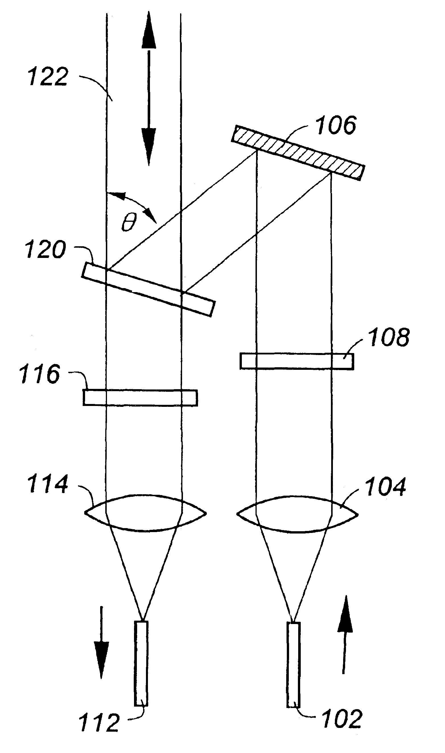
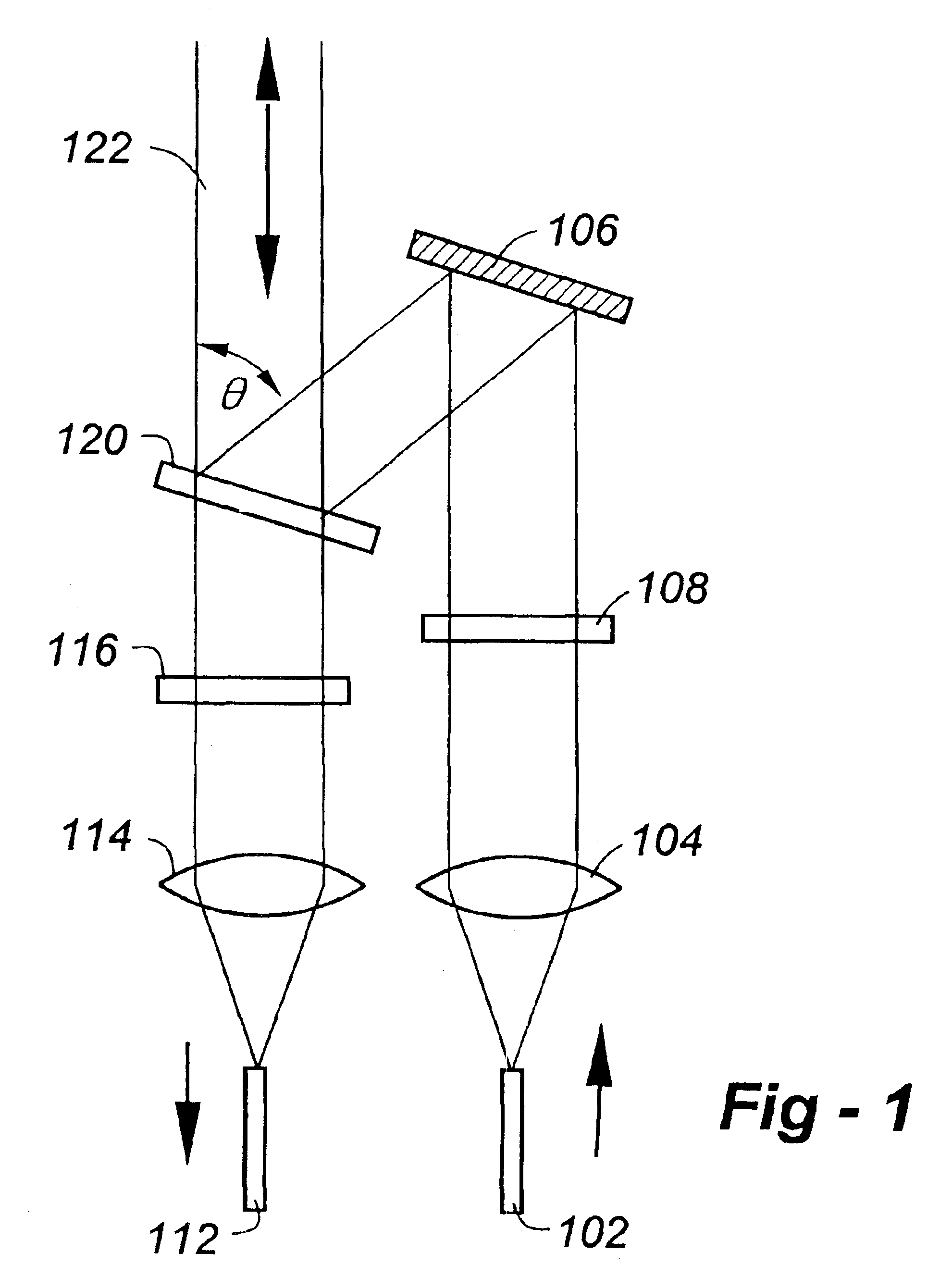
[0011]FIG. 1 is a diagram which shows the preferred embodiment of the invention. Excitation illumination is brought into the probe over fiber 102, which is then collimated by lens 104. The collimated light then passes through a bandpass filter 108 to remove the non-laser wavelengths generated en route from the source. In contrast to previous designs, which rely exclusively on holographic optical elements, this invention uses a dielectric component, at least the bandpass filter 108, since this allows the element to be fabricated in a more compact size using existing technology. The filtered light is reflected by a mirror 106 onto a beam combiner 120 which is then directed to a sample along a counter-propagating path 122. The light scattered by the sample under investigation returns along path 122, passes through beam combiner 120, and is filtered by an optional notch filter 116 before being focused by lens 114 onto the end of collection fiber 112. Although the beam combiner 120 and o...
PUM
| Property | Measurement | Unit |
|---|---|---|
| angle | aaaaa | aaaaa |
| excitation energy | aaaaa | aaaaa |
| energy | aaaaa | aaaaa |
Abstract
Description
Claims
Application Information

