Silicon Interposer Sandwich Structure for ESD, EMC, and EMC Shielding and Protection

a technology of emc and emc, which is applied in the direction of semiconductor devices, semiconductor/solid-state device details, electrical devices, etc., can solve the problem of reducing the enhancement of functional proximity otherwise afforded by the interposer tsv 3d packaging, and achieves the effect of rapid heat dissipation of the integrated circuit devi

Pending Publication Date: 2021-09-16
IBM CORP
View PDF5 Cites 0 Cited by
  • Summary
  • Abstract
  • Description
  • Claims
  • Application Information

AI Technical Summary

Benefits of technology

[0021]The top interposer has a blanket metal coating on the bottom or top surface and the connections to the bottom interposer or the chip carrier would be to electrical ground or bias depending on the function required. As shown in FIG. 2, one or more devices connected to the bottom interposer may be shielded with a top interposer selectively to provide the functional isolation for shielding or protection desired, for maximum miniaturization. Thermal interface material can be dispensed on the back of the integrated circuit device prior to joining the top interposer in order to provide for rapid heat dissipation from the integrated circuit device if required.

Problems solved by technology

These would be constructed with base plates, lids, gaskets, and device separation common in the industry for shielding and protection but this defeats the enhancement of functional proximity otherwise afforded by the interposer TSV 3D packaging.

Method used


Image

  • Silicon Interposer Sandwich Structure for ESD, EMC, and EMC Shielding and Protection
  • Silicon Interposer Sandwich Structure for ESD, EMC, and EMC Shielding and Protection

Examples


Embodiment Construction

[0024]To achieve the foregoing and other advantages, and in accordance with the purpose of this invention as embodied and broadly described herein, the following detailed description comprises disclosed examples of the invention that can be embodied in various forms.

[0025]The specific processes, compounds, compositions, and structural details set out herein not only comprise a basis for the claims and a basis for teaching one skilled in the art to employ the present invention in any novel and useful way, but also provide a description of how to make and use this invention. The written description, claims, abstract of the disclosure, and the drawings that follow set forth various features, objectives, and advantages of the invention and how they may be realized and obtained. These features, objectives, and advantages will also become apparent by practicing the invention.

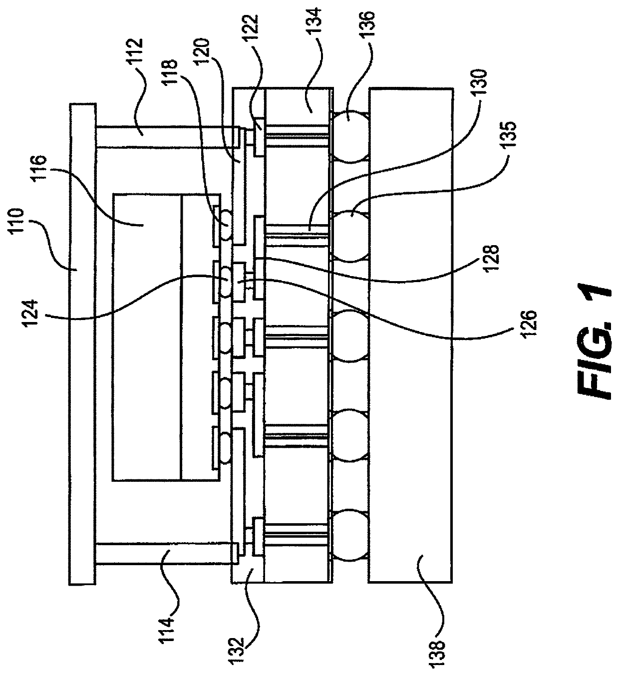
[0026]As noted before, the interposer sandwich structure as shown in FIG. 1 comprises two interposers enclosing a d...


PUM

PropertyMeasurementUnit
heightsaaaaaaaaaa
Electromagnetic Conductivityaaaaaaaaaa
capacitanceaaaaaaaaaa

Abstract

An interposer sandwich structure includes a top interposer and a bottom interposer enclosing an integrated circuit electronic device that includes an attachment for attaching the device to the bottom interposer, and an interconnection structure connecting the top interposer to the bottom interposer. The top interposer may also be directly connected to a chip carrier in addition to the bottom interposer. The structure provides shielding and protection of the device against Electrostatic Discharge (ESD), Electromagnetic Interference (EMI), and Electromagnetic Conductivity (EMC) in miniaturized 3D packaging.

Description

CROSS-REFERENCE TO RELATED APPLICATIONS[0001]This application is a continuation of U.S. patent application Ser. No. 15 / 688,369 filed Aug. 28, 2017, which is in turn a continuation of U.S. patent application Ser. No. 15 / 131,171 filed Apr. 18, 2016, which is in turn a continuation of U.S. patent application Ser. No. 13 / 251,987 filed Oct. 3, 2011. The complete disclosures of U.S. patent application Ser. No. 15 / 688,369, U.S. patent application Ser. No. 15 / 131,171, and U.S. patent application Ser. No. 13 / 251,987 are all hereby expressly incorporated herein by reference in their entireties for all purposes.BACKGROUND[0002]The field of the invention comprises miniaturization of electronics through 3D packaging structures incorporating integrated circuit devices protected against Electrostatic Discharge (ESD), Electromagnetic Interference (EMI), and Electromagnetic Conductivity (EMC)[0003]Miniaturization of electronics is a continuously evolving process in devices generated today. One way o...

Claims


Application Information

Patent Timeline
Patent Type & Authority Applications(United States)
IPC IPC(8): H01L23/00H01L23/552H01L23/498H01L25/065H01L23/367H01L23/60
CPCH01L24/81H01L2924/1579H01L23/49827H01L25/0655H01L23/367H01L23/49816H01L23/49833H01L23/60H01L24/09H01L2924/1461H01L2224/16225H01L2924/15192H01L2924/15311H01L2924/19105H01L2224/08238H01L2224/81192H01L2924/01014H01L2924/01028H01L2924/01029H01L2924/01047H01L2924/0105H01L2924/01082H01L2924/014H01L2924/14H01L2924/1433H01L2924/15331H01L2924/15738H01L2924/15787H01L23/552H01L2924/00
Inventor BERNIER, WILLIAM EMMETTDANG, BINGKNICKERBOCKER, JOHNTRAN, SON KIMINTERRANTE, MARIO J.
Owner IBM CORP
Why Eureka
Try Eureka