Semiconductor device and method of fabricating the same

a semiconductor and device technology, applied in the direction of transistors, vacuum evaporation coatings, coatings, etc., can solve the problems of reducing the reliability of tft, unsuitable for using noncrystalline silicon films as active layers, etc., and achieve the effect of quick dissipation of heat generated

Inactive Publication Date: 2005-05-10
SEMICON ENERGY LAB CO LTD
View PDF33 Cites 34 Cited by
  • Summary
  • Abstract
  • Description
  • Claims
  • Application Information

AI Technical Summary

Benefits of technology

[0010]The present invention has been made in view of the foregoing problem, and therefore has an object to provide a technique for equalizing a heat distribution all over a semiconductor device by quickly dissipating heat generated when a TFT provided on an insulating surface is driven.
[0013]In order to attain the foregoing objects, the present invention is characterized in that an insulating film (SiNxByOz: where, X, Y and Z are values expressing the composition ratio, and X>0, Y>0, and Z>0) superior in thermal conductivity, which is formed by using a sputtering method in which film formation can be made at a low temperature and productivity is superior, is used as an insulating film of a semiconductor component or a semiconductor device. Since the insulating film (SiNxByOz) of the present invention contains boron of 0.1 to 50 atoms % or 1 to 50 atoms %, preferably 1 to 10 atoms %, the film has high thermal conductivity, and has an effect to prevent deterioration of characteristics due to heat of a semiconductor device. Moreover, since the insulating film (SiNxByOz) of the present invention has a blocking effect to movable ions such as sodium, the film has also an effect to prevent these ions from intruding into the semiconductor device, especially into a channel formation region from the substrate or the like. In addition, since the insulating film (SiNxByOz) of the present invention contains oxygen of 1 to 30 atoms %, the internal stress of the film can be made typically −5×10¹⁰ dyn / cm2 to 5×10¹⁰ dyn / cm2, preferably −1010 dyn / cm2 to 1010 dyn / cm2, stresses of the respective films are reduced, and it is possible to make film peeling hard to cause.

Problems solved by technology

Since the driver circuit or the logic circuit of the active matrix type liquid crystal display device is required to perform a high speed operation, it is unsuitable to use a noncrystalline silicon film (amorphous silicon film) as an active layer.
In such an active matrix type display device, especially in the case where a TFT is provided on a substrate (for example, a glass substrate) having bad thermal conductivity and good heat retaining property, since a large voltage and current is applied to a TFT of a peripheral driver circuit, a semiconductor layer generates heat and remarkably lowers the reliability of the TFT.

Method used


Image

  • Semiconductor device and method of fabricating the same
  • Semiconductor device and method of fabricating the same
  • Semiconductor device and method of fabricating the same

Examples


embodiment 1

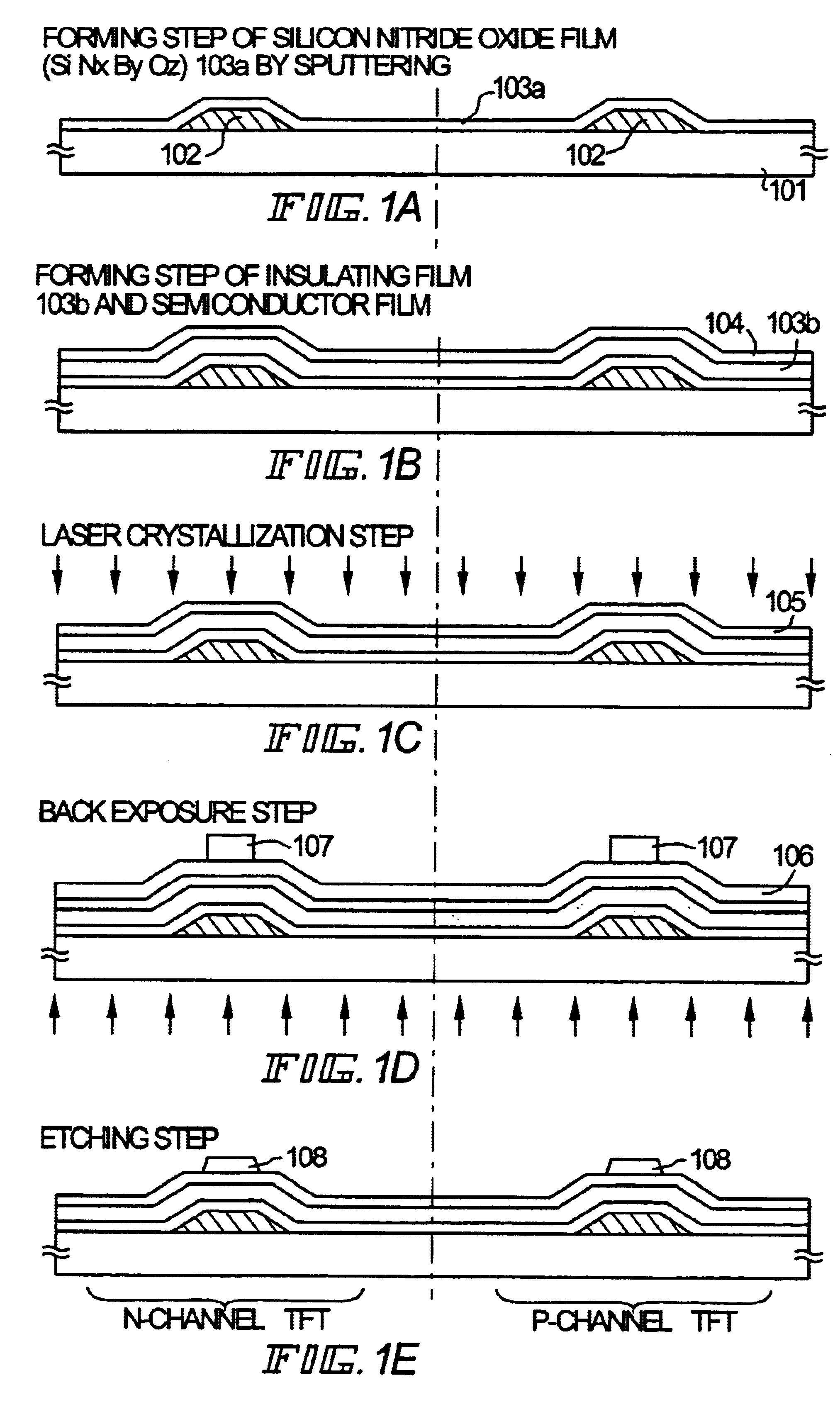
[0087]An embodiment of the present invention will be described below with reference to FIGS. 1A to 3D.

[0088]First, as a substrate 101, a glass substrate (Corning 1737; distortion point 667° C.) was prepared. Next, a gate wiring line (including a gate electrode) 102 of a laminate structure (not shown for simplification) was formed on the substrate 101. In this embodiment, a sputtering method was used to form a laminate of a tantalum nitride film (thickness of 50 nm) and a tantalum film (thickness of 250 nm), and the gate wiring line (including the gate electrode) 102 having the laminate structure was formed by using a photolithography method of a well-known patterning technique.

[0089]Next, a silicon nitride oxide film (SiNxByOz) 103a having a thickness of 1 to 1000 nm, preferably 10 to 100 nm and containing boron was formed (FIG. 1A). In this embodiment, sputtering using a target of single crystal silicon added with boron was carried out in an atmosphere containing nitric oxide gas (...

embodiment 2

[0103]In Embodiment 1 , the amorphous silicon film was crystallized by laser light. In this embodiment, a description will be made on an example in which crystallization of an amorphous semiconductor film is carried out by a method different from Embodiment 1. This embodiment will be described below with reference to FIGS. 4A to 6D.

[0104]First, a gate electrode 102 and gate insulating films 103a and 103b were formed on a substrate 101 similarly to Embodiment 1(FIG. 4A). Since steps up to this are the same as Embodiment 1, the same reference numerals are used. The gate insulating film 103a is a silicon nitride oxide film (SiNxByOz) containing boron.

[0105]Next, in accordance with Embodiment 1, an amorphous silicon film 104a was formed. Next, by irradiation of UV light in an oxygen atmosphere, a not-shown very thin oxide film was formed on the surface of the amorphous silicon film 104a. This oxide film has a function to improve wettability of a solution containing nickel applied later....

embodiment 3

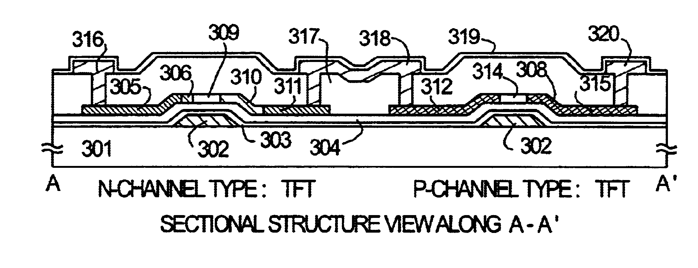
[0127]An example of a semiconductor device including an n-channel TFT and a p-channel TFT using the fabricating steps of Embodiment 1 or Embodiment 2 will be described with reference to FIGS. 7A to 7C and FIGS. 8A and 8C.

[0128]The semiconductor device of this embodiment of the present invention includes a peripheral driver circuit portion and a pixel matrix circuit portion on the same substrate. In this embodiment, for simplification of illustration, a CMOS circuit constituting a part of the peripheral circuit portion is shown in FIGS. 7A to 7C, and a pixel TFT (N-channel TFT) constituting a part of the pixel matrix circuit portion is shown in FIGS. 8A and 8B. In addition to the fabricating steps of Embodiments 1 and 2, a passivation film (protecting film) 319 of 0.2 to 0.4 μm was formed. As the passivation film 319, it is preferable to make such a structure that a silicon nitride film, for example, the silicon nitride oxide film (SiNxByOz) containing boron is used to prevent deteri...


PUM

PropertyMeasurementUnit
thicknessaaaaaaaaaa
thicknessaaaaaaaaaa
thicknessaaaaaaaaaa

Abstract

A semiconductor device using a TFT structure with high reliability is realized. As an insulating film used for the TFT, for example, a gate insulating film, a protecting film, an under film, an interlayer insulating film, or the like, a silicon nitride oxide film (SiNXBYOz) containing boron is formed by a sputtering method. As a result, the internal stress of this film becomes −5×10¹⁰ dyn / cm2 to 5×10¹⁰ dyn / cm2, preferably −1010 dyn / cm2 to 1010 dyn / cm2, and the film has high thermal conductivity, so that it typically becomes possible to prevent deterioration due to heat generated at the time of an on operation of the TFT.

Description

BACKGROUND OF THE INVENTION[0001]1. Field of the Invention[0002]The present invention relates to a method of fabricating a semiconductor device using a crystalline semiconductor film formed by crystallizing an amorphous semiconductor thin film, and particularly to a method of improving reliability of a semiconductor device. The semiconductor device of the present invention includes not only a component such as a thin film transistor (TFT) or a MOS transistor but also an electro-optical device such as a display device or an image sensor including a semiconductor circuit constituted by such insulated gate transistors. In addition, the semiconductor device of the present invention includes an electronic equipment incorporating such a display device and an electro-optical device.[0003]2. Description of the Related Art[0004]In recent years, a technique for constructing a semiconductor circuit by forming TFTs on a glass substrate or the like has been rapidly developed. As such a semicondu...

Claims


Application Information

Patent Timeline
Patent Type & Authority Patents(United States)
IPC IPC(8): H01L21/02H01L21/336H01L21/70H01L29/66H01L21/314H01L29/786H01L21/84H01L27/12H01L29/49H01L29/40C23C14/00C23C14/06H01L21/77
CPCC23C14/0057C23C14/06H01L21/3143H01L21/3144H01L29/78678H01L29/4908H01L29/66765H01L29/78606H01L29/78669H01L27/1214H01L27/1203H01L27/1259H01L21/02266H01L21/02126
Inventor YAMAZAKI, SHUNPEI
Owner SEMICON ENERGY LAB CO LTD
Why Eureka
Try Eureka