Method and device for detecting wafer surface defects

A detection method and defect technology, applied in the direction of measuring devices, optical devices, semiconductor/solid-state device testing/measurement, etc., can solve problems such as inaccurate positioning, inability to locate chips, unfavorable analysis, etc.

Active Publication Date: 2011-05-11
CSMC TECH FAB2 CO LTD
View PDF1 Cites 13 Cited by
  • Summary
  • Abstract
  • Description
  • Claims
  • Application Information

AI Technical Summary

Problems solved by technology

However, when the above-mentioned equipment is used for inspection, the size of the test strip should not be less than 2mm×2mm. Therefore, when the size of the chip is smaller than 2mm, one test strip will include the area w...

Method used


Image

  • Method and device for detecting wafer surface defects
  • Method and device for detecting wafer surface defects
  • Method and device for detecting wafer surface defects

Examples


Embodiment Construction

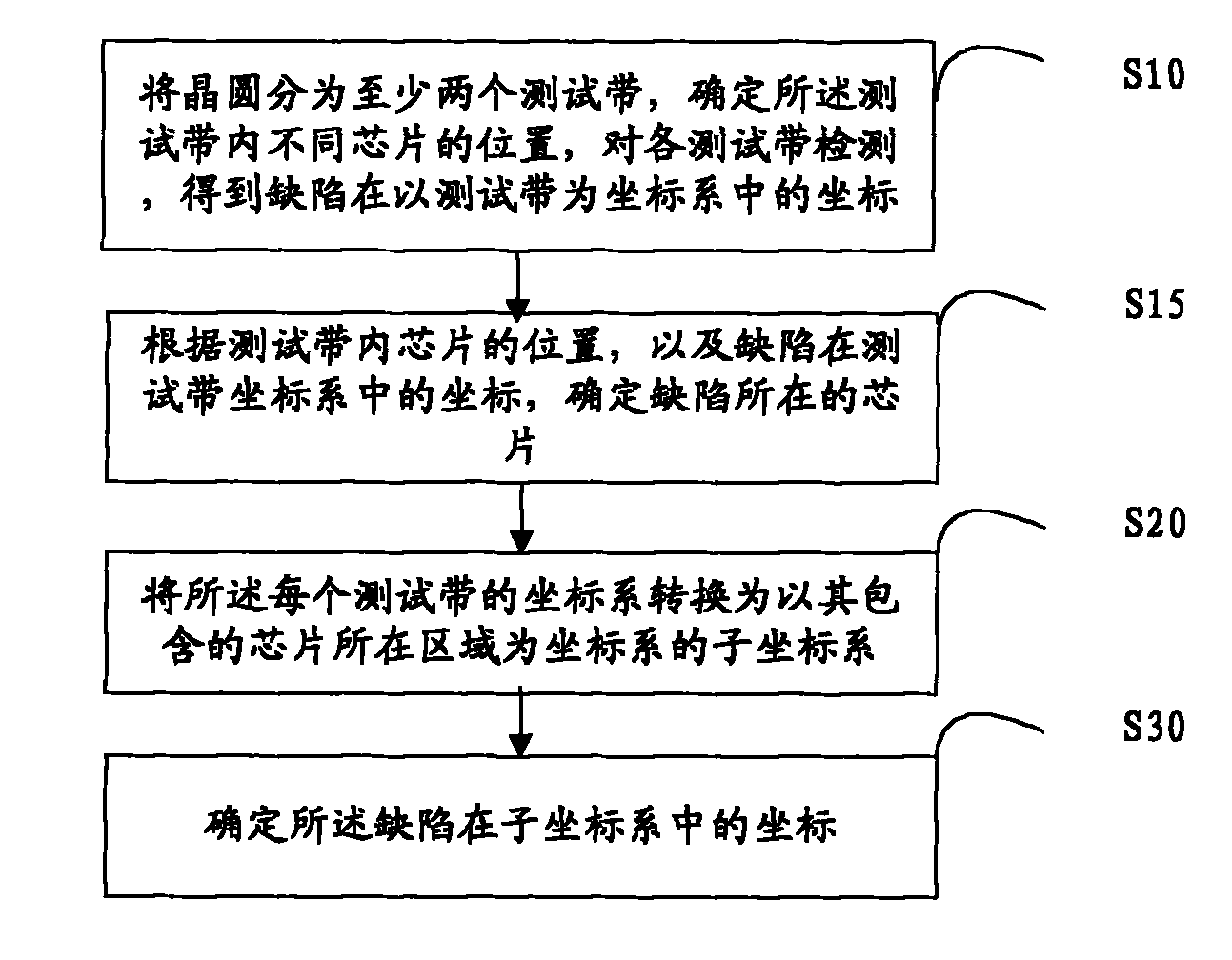
[0029] It can be seen from the background technology that an existing detection device for detecting defects on the surface of a wafer uses a test tape (die by die) comparison method to detect defects. However, the usual size of a test tape can be one chip (chip) The area where the chip is located or the area where multiple chips are located, or an exposure area (BLOCK), the result file generated by the detection corresponds to the defined test zone, so that the position of the defect in the test zone can be located. However, when the above-mentioned equipment is used for inspection, the size of the test strip should not be less than 2mm×2mm. Therefore, when the size of the chip is smaller than 2mm, one test strip will include the area where multiple chips are located, so that the equipment cannot accurately locate the defect. The position in the chip, so that the chip with the defect cannot be located, so it is not conducive to analyzing the cause of the defect.

[0030] Ther...


PUM


Abstract

The invention discloses a method and device for detecting wafer surface defects. The method comprises the steps of: diving a wafer into at least two test tapes, determining the positions of different chips in the test tapes, and detecting the test tapes respectively to obtain the coordinates of the defects in test tape coordinate systems with the test tapes as coordinate systems; determining the chips in which the defects are located according to the positions of the chips in the test tapes and the coordinates of the defects in the test tape coordinate systems; converting the coordinate system of each test tape into a subcoordinate system with an area, in which the chip contained by the corresponding test tape is located, as a coordinate system; and determining the coordinates of the defects in the subcoordiante systems. The method and device can be used for positioning the positions of the defects in the chips.

Description

technical field [0001] The invention relates to the technical field of semiconductor manufacturing, in particular to a method and device for detecting wafer surface defects. Background technique [0002] The size of semiconductor chips is getting smaller and smaller, and the impact of defects in the process on the yield is becoming more and more obvious. Accurate analysis of defects is directly related to the judgment of chip failure and the improvement direction of defects. [0003] The current defect analysis equipment used for mainstream 6-inch wafers uses a die by die comparison method to detect defects when analyzing the wafers. [0004] For example, a method for detecting wafer defects is disclosed in Chinese patent literature with the application number "200710045485". The method for detecting wafer defects includes the following steps: selecting a detection zone, the detection zone is centered on the center of the wafer , the radius is a circular area of ​​one-tent...

Claims


Application Information

Patent Timeline
IPC IPC(8): H01L21/66G01B11/03
Inventor 顾颂
Owner CSMC TECH FAB2 CO LTD
Why Eureka
Try Eureka