System chip JTAG (Joint Test Action Group) debugging control method based on chip flash memory

A system chip and control method technology, applied in the direction of measuring devices, instruments, measuring electronics, etc., can solve problems such as data security risks and poor security, and achieve the effects of improving security, facilitating debugging, and protecting data security

Active Publication Date: 2011-05-25
C SKY MICROSYST CO LTD
View PDF4 Cites 19 Cited by
  • Summary
  • Abstract
  • Description
  • Claims
  • Application Information

AI Technical Summary

Problems solved by technology

[0012] In order to overcome the deficiencies of existing system chip JTAG debugging control methods that have hidden dangers in data security and poor security, the present invention provides a system chip JTAG debugging based on on-chip flash memory that ensures data security and improves security while facilitating debugging. Control Method

Method used


Image

  • System chip JTAG (Joint Test Action Group) debugging control method based on chip flash memory
  • System chip JTAG (Joint Test Action Group) debugging control method based on chip flash memory
  • System chip JTAG (Joint Test Action Group) debugging control method based on chip flash memory

Examples


Embodiment Construction

[0041] The present invention will be further described below in conjunction with the accompanying drawings.

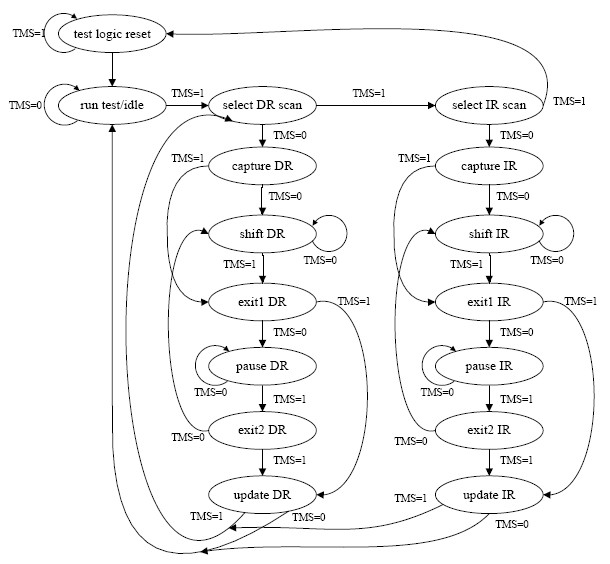
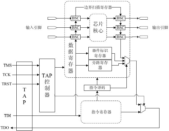
[0042] refer to Figure 3 ~ Figure 5 , a system chip JTAG debugging control method based on on-chip flash memory, the JTAG realizes the control of the boundary scan chain through TAP, and the TAP interface includes a TCK interface, a TMS interface, a TDI interface, a TDO interface and a TRST interface, and the TCK The interface, TMS interface and TDI interface are respectively controlled by a two-choice data selector. The two inputs of the data selector are normal signal and fixed low level or high level respectively, and then through a bit in the system chip The register REG1 with a width of one bit is used to control the data selector. When the value of the register REG1 is one, the low-level signal is connected to the TCK interface, the TMS interface and the TDI interface, and the JTAG interface is shielded; while the value of the register REG1 is zero. , connect t...


PUM


Abstract

The invention discloses a system chip JTAG (Joint Test Action Group) debugging control method based on a chip flash memory. A JTAG realizes control on a boundary scanning chain through a TAP (Test Access Port), a TCK (Test Clock) interface, a TMS (Time Multiplexed Switching) interface and a TDI (Transport Driver Interface) are respectively controlled by an alternative datum, two inputs of a data selector are respectively used as a normal signal and a fixed low level or high level, the data selector is controlled through a register REG 1 with a bit width of a bit in a system chip, when the value of the REG1 is 1, the low level is connected to the TCK interface, the TMS interface and the TDI through signals and used for shielding an JTAG interface; when the value of the REG1 is 0, the normal signal is connected to the TCK interface, the TMS interface and the TDI and enters a normal debugging mode; and the value of the REG1 is determined according to the data of the chip flash memory. The invention ensures the data security and improves the security while the debugging is convenient.

Description

technical field [0001] The invention relates to the field of system chips, in particular to a system chip JTAG debugging control method. Background technique [0002] System on Chip (SOC, System on Chip) refers to the integration of a complete system on a single chip. This design technique began in the mid-1990s. With the rapid development of semiconductor process technology, IC (Integrated Circuit, integrated circuit) designers can integrate more and more complex functions into a single silicon chip, and integrated circuits (IC) to integrated systems (IS, Integrate System) have emerged. The trend of change, SOC is produced under this change. With the maturity of deep submicron process technology, the scale of integrated circuit chips is getting larger and larger. Digital IC has developed from a timing-driven design method to a design method based on IP (Intellectual Property, intellectual property) core multiplexing, which is widely used in SOCs. SOC can make full use o...

Claims


Application Information

Patent Timeline
Patent Type & Authority Applications(China)
IPC IPC(8): G01R31/3185
Inventor 严晓浪曾健林黄凯葛海通
Owner C SKY MICROSYST CO LTD
Why Eureka
Try Eureka