Supercharge Your Innovation With Domain-Expert AI Agents!

Domain structure of memory circuit

A technology of memory circuit and layout structure, which is applied to circuits, electrical components, electric solid-state devices, etc., and can solve problems such as time-consuming search and error-prone

Inactive Publication Date: 2011-06-08
SHANGHAI HUA HONG NEC ELECTRONICS
View PDF0 Cites 1 Cited by
  • Summary
  • Abstract
  • Description
  • Claims
  • Application Information

AI Technical Summary

Problems solved by technology

Sometimes it is necessary to find the failed memory cell on the circuit layout to analyze the cause of its failure, and if there are many memory cells in the memory circuit, for example, thousands of rows × thousands of columns, engineers need to spend a long time to find failed memory cells and are prone to error

Method used


Image

  • Domain structure of memory circuit
  • Domain structure of memory circuit
  • Domain structure of memory circuit

Examples


Embodiment Construction

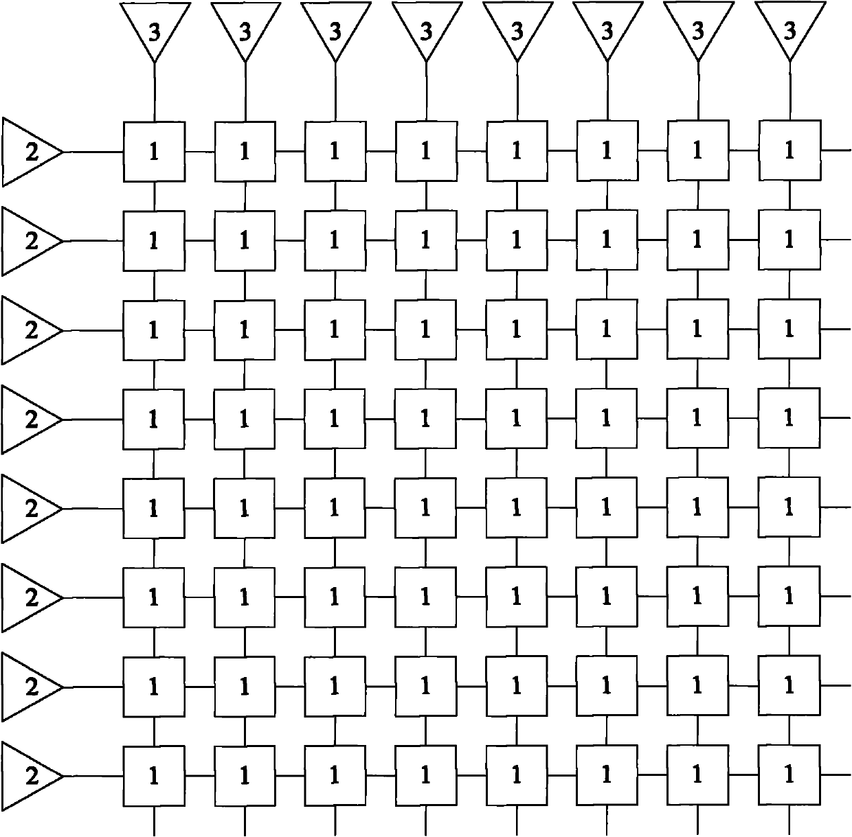
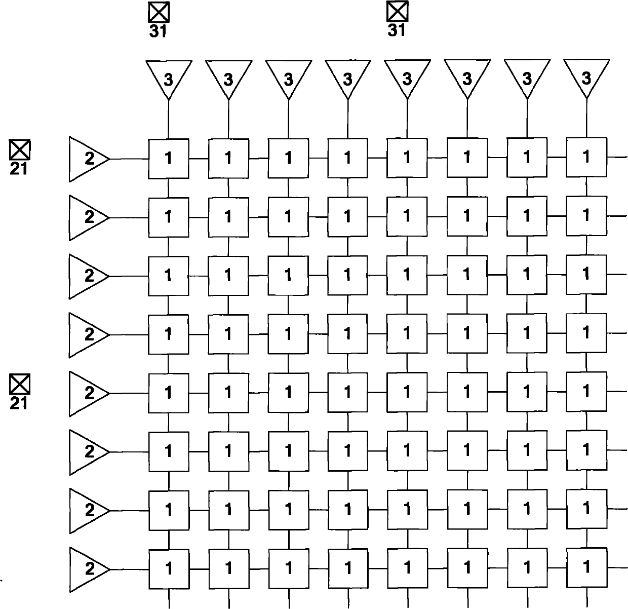
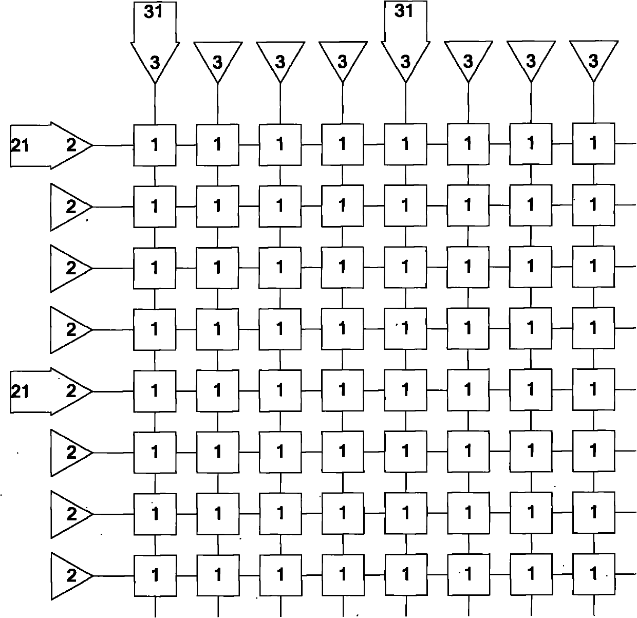
[0014] see figure 2 , which is a schematic diagram of the layout structure of the memory circuit in the present invention. The memory circuit includes a memory array formed by memory cells 1 , a row selection circuit 2 , and a column selection circuit 3 . The innovation of the present invention is that: every equal number of rows, there is a row mark 21 in the open area next to the row of the memory circuit layout; The adjacent clear area has a column marker 31 .

[0015] figure 2 In the middle, a row mark 21 is designed every 4 rows, that is, a row mark 21 is designed in the open area next to the 1st row, the 5th row...; a column mark 31 is designed every 4 columns, that is, it is close to the 1st Column 5... Design column flag 31 for the empty area next to it. The open area refers to a useless area that does not have any impact on the function and use of the circuit. Utilizing these useless areas will not result in an additional increase in the total area of ​​the cir...


PUM


Abstract

The invention discloses a domain structure of a memory circuit. The memory circuit comprises a memory array formed by arraying memory units, a row selection circuit and a column selection circuit; a row sign is arranged on the margin next to the row of the memory circuit domain every equal number of rows; and a column sign is arranged on a margin next to the column of the memory circuit domain every equal number of columns. The domain structure of the memory circuit can help engineers locate the actual position of the memory unit quickly and exactly, so the searching time is obviously reduced, error probability is lowered, and a powerful basis for the analysis of ineffectiveness factor is provided.

Description

technical field [0001] The invention relates to a semiconductor integrated circuit layout design structure. Background technique [0002] Semiconductor integrated circuit products usually contain memory circuits. An important feature of memory circuits is that the smallest unit of memory cells is evenly arranged in an array with the same orientation or pairwise symmetrical orientation and the same spacing, usually in a rectangular arrangement. [0003] see figure 1 , which is a schematic layout of a memory circuit, including a memory array and peripheral circuits. A plurality of storage units 1 are arranged as a rectangular memory array, wherein each storage unit 1 has a uniquely determined electrical address corresponding to it. Each row of storage units 1 is connected to a row selection circuit 2 , and each column of storage units 1 is connected to a column selection circuit 3 . The row selection circuit 2 and the column selection circuit 3 mainly constitute peripheral ...

Claims


Application Information

Patent Timeline
IPC IPC(8): H01L27/10
Inventor 张雨田曾志敏章成嘉
Owner SHANGHAI HUA HONG NEC ELECTRONICS
Features
  • R&D
  • Intellectual Property
  • Life Sciences
  • Materials
  • Tech Scout
  • Unparalleled Data Quality
  • Higher Quality Content
  • 60% Fewer Hallucinations
Learn More