Improved band-gap reference voltage source and band-gap reference voltage generating circuit

A reference voltage source and reference voltage technology, applied in the direction of adjusting electrical variables, control/regulating systems, instruments, etc., can solve the problems of transistor current i cannot be completely matched, voltage offset, and drain voltages are not uniform, to avoid Voltage offset problem, reduce current jitter, improve the effect of suppression

Active Publication Date: 2015-05-20
SHANGHAI INTEGRATED CIRCUIT RES & DEV CENT
View PDF5 Cites 0 Cited by
  • Summary
  • Abstract
  • Description
  • Claims
  • Application Information

AI Technical Summary

Problems solved by technology

[0003] Although the traditional bandgap reference voltage generation circuit can obtain a relatively high power supply rejection ratio by adding a regulator, the circuit has the following disadvantages: 1. The drain voltages of the PMOS transistors M3 and M4, and the NMOS transistors M1 and M2 are inconsistent It will cause the currents passing through them to not be completely matched; 2. The added regulator 103 will introduce a voltage offset of the circuit, which increases the difficulty of design
[0004] To sum up, it can be seen that the bandgap reference voltage generating circuit of the prior art has the problems that the currents flowing through each transistor cannot be completely matched and the voltage offset will be generated. Therefore, it is necessary to propose an improved technical means to solve this problem. a question

Method used


Image

  • Improved band-gap reference voltage source and band-gap reference voltage generating circuit
  • Improved band-gap reference voltage source and band-gap reference voltage generating circuit
  • Improved band-gap reference voltage source and band-gap reference voltage generating circuit

Examples


Embodiment Construction

[0014] The following describes the implementation of the present invention through specific specific examples in conjunction with the accompanying drawings. Those skilled in the art can easily understand other advantages and effects of the present invention from the content disclosed in this specification. The present invention can also be implemented or applied through other different specific examples, and various details in this specification can also be based on different viewpoints and applications, and various modifications and changes can be made without departing from the spirit of the present invention.

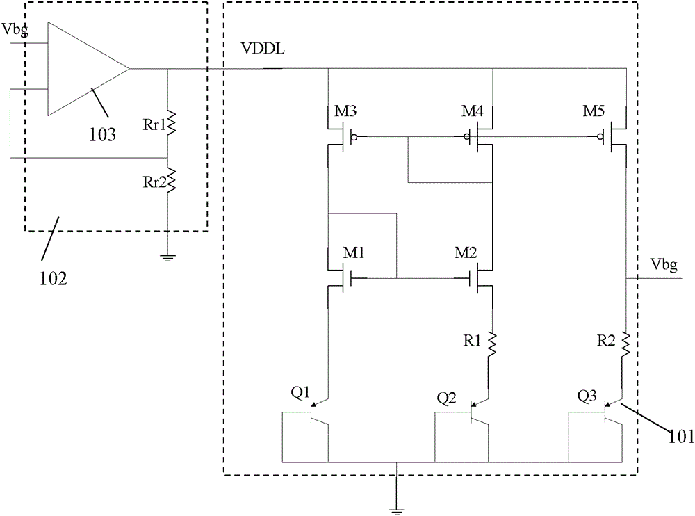
[0015] figure 2 It is a schematic diagram of the circuit structure of a preferred embodiment of an improved band gap reference voltage source of the present invention. Such as figure 2 As shown, an improved bandgap reference voltage source of the present invention includes at least a first NMOS transistor M1 and a second NMOS transistor M2 connected to the gates, a thi...


PUM


Abstract

The invention provides an improved band-gap reference voltage source and a band-gap reference voltage generating circuit. The band-gap reference voltage generating circuit comprises the improved band-gap reference voltage source and a cascade current mirror circuit. The band-gap reference voltage generating circuit feeds current back to the positive power supply input end of the improved band-gap reference voltage source through the cascade current mirror circuit. Simultaneously, in the improved band-gap reference voltage source, a P type metal-oxide-semiconductor field-effect transistor (MOSFET) is arranged between a power supply end and the conventional improved band-gap reference voltage source, so that the impedance of the power supply input end is approximately the transimpedance of the MOSFET and the power supply suppression ratio of the power supply is increased. Moreover, two resistors are arranged in the improved band-gap reference voltage source on the basis of the conventional improved band-gap reference voltage source, so that drain end voltage of two groups of symmetrical tubes of a differential circuit is closer to each other and current is better matched simultaneously.

Description

Technical field [0001] The invention relates to a bandgap reference voltage source and a bandgap reference voltage generating circuit, in particular to an improved bandgap reference voltage source and a bandgap reference voltage generating circuit with high power supply rejection ratio and better matching of MOS differential pair tube currents Circuit. Background technique [0002] Because of its low temperature coefficient characteristics, the band gap reference voltage source is widely used in various analog and mixed signal circuit systems. Accordingly, the band gap reference voltage has become an indispensable part of analog and mixed signal circuit systems. figure 1 It is a circuit structure diagram of a traditional bandgap reference voltage generating circuit. As shown in the figure, the conventional bandgap reference voltage generating circuit includes a conventional bandgap reference voltage source 101 and a regulator 102, where the conventional bandgap reference voltage ...

Claims


Application Information

Patent Timeline
Patent Type & Authority Patents(China)
IPC IPC(8): G05F3/24
Inventor 任铮胡少坚周伟
Owner SHANGHAI INTEGRATED CIRCUIT RES & DEV CENT
Why Eureka
Try Eureka