Semiconductor package and manufacturing method thereof

A package and semiconductor technology, applied in the fields of semiconductor/solid-state device manufacturing, semiconductor devices, semiconductor/solid-state device components, etc., can solve the problems of high-frequency chip interconnection limitations, poor heat dissipation performance of LOC packages, and high equipment costs

Inactive Publication Date: 2011-06-15
SAMSUNG SEMICON CHINA RES & DEV +1
View PDF0 Cites 2 Cited by
  • Summary
  • Abstract
  • Description
  • Claims
  • Application Information

AI Technical Summary

Problems solved by technology

[0004] The traditional LOC package uses the gold wire bonding method to interconnect the chip with the pins of the lead frame, which has the following disadvantages: the cost of

Method used


Image

  • Semiconductor package and manufacturing method thereof
  • Semiconductor package and manufacturing method thereof
  • Semiconductor package and manufacturing method thereof

Examples


Embodiment Construction

[0020] The semiconductor package and its manufacturing method according to the present invention use conductive elements instead of traditional gold wires to electrically connect the chip pads to the leads of the lead frame, thereby realizing the interconnection between the chip pads and the leads.

[0021] Hereinafter, embodiments of the present invention will be described in detail with reference to the accompanying drawings.

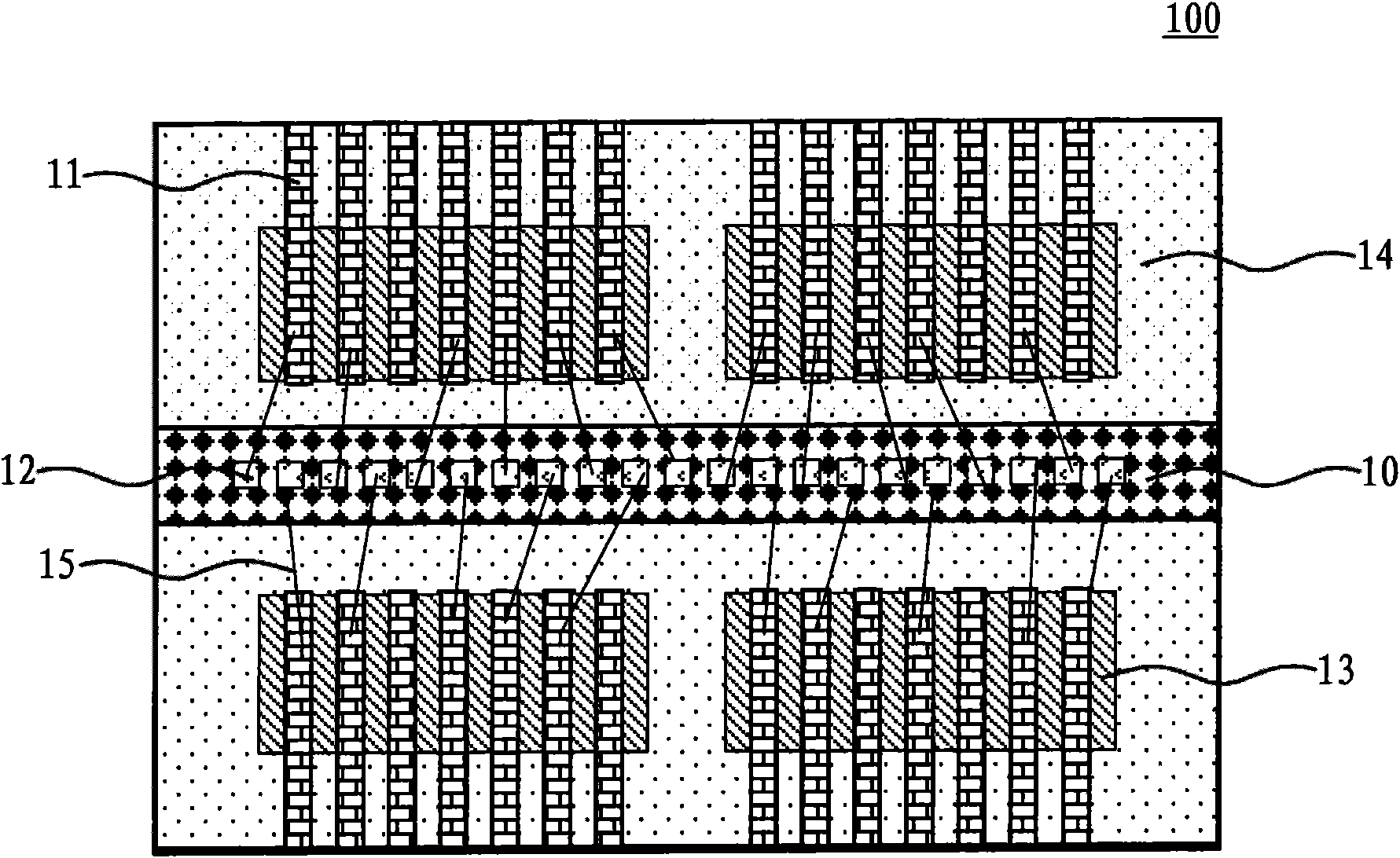
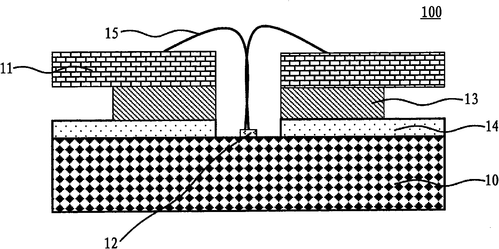
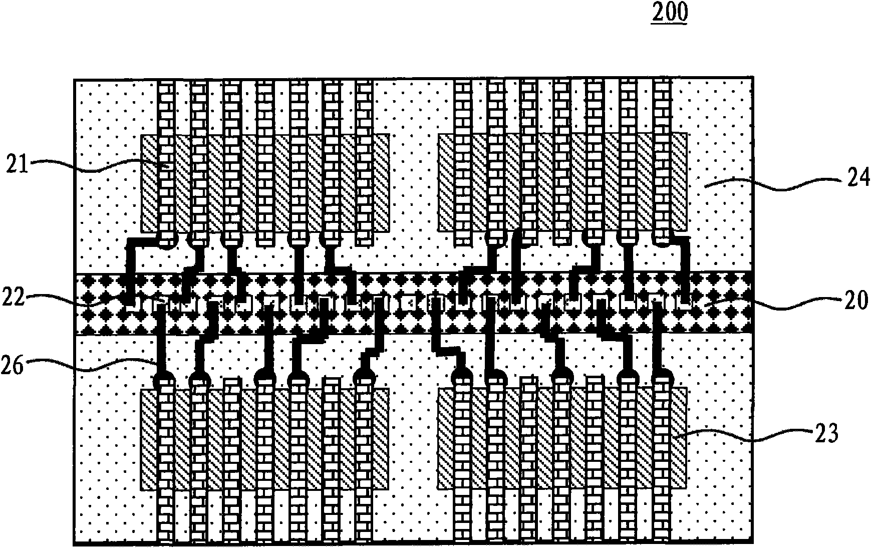
[0022] refer to image 3 and Figure 4 , the LOC package 200 according to the first exemplary embodiment of the present invention includes: a chip 20; a chip surface protection layer 24, formed above the chip 20, covering the area of ​​the chip 20 except the area where the chip pad 22 will be formed; The chip pad 22 is formed on the area of ​​the chip 20 that is not covered by the chip surface protection layer 24; the LOC tape 23 is formed on the chip surface protection layer 24; the pin 21 is formed on the LOC tape 23 and passed through the LOC tape...


PUM


Abstract

The invention discloses a semiconductor package and a manufacturing method thereof. The semiconductor package comprises a chip, chip surface protecting layers, chip bonding pads, lead on chip (LOC) tapes, pins, conducting components and resins, wherein the chip surface protecting layers are formed on the chip and cover the areas except the areas in which the chip bonding pads are about to form; the chip bonding pads are formed in the areas, which are not covered by the chip surface protecting layers, on the chip; the LOC tapes are formed on the chip surface protecting layers; the pins are formed on the LOC tapes which bond the pins and the chip surface protecting layers; the conducting components are formed on the chip bonding pads and part of the chip surface protecting layers and connect the chip bonding pads with the pins electrically; and the resins are used for packaging the components.

Description

technical field [0001] The invention relates to a semiconductor package and a manufacturing method thereof. More particularly, the present invention relates to a semiconductor package using conductive elements to interconnect chip pads with leads of a lead frame and a method of manufacturing the same. Background technique [0002] With the development of semiconductor packaging technology, higher requirements are put forward for the reliability and heat dissipation of the semiconductor package. figure 1 A schematic diagram of a lead on chip (LOC) package according to the prior art is shown. figure 2 shows that according to the prior art figure 1 A cross-sectional view of the LOC package shown in . [0003] refer to figure 1 and figure 2 , the semiconductor package 100 according to the prior art includes: a chip 10; a chip surface protection layer 14, formed above the chip 10, covering the area of ​​the chip 10 except the area where the chip pad 12 will be formed; the ...

Claims


Application Information

Patent Timeline
IPC IPC(8): H01L23/488H01L23/485H01L21/60
CPCH01L2224/32225H01L2224/4824H01L24/82H01L2224/73215H01L2224/48091H01L2924/00014H01L2924/00
Inventor 陈强
Owner SAMSUNG SEMICON CHINA RES & DEV
Why Eureka
Try Eureka