Chip picking and position aligning confirmation method for ink dot-free test

An ink dot and testing machine technology, which is applied in the field of non-ink dot test pick sheet alignment confirmation, can solve the problems of error-prone, multi-sized chips, and difficulty in the latter, so as to reduce the difficulty of confirmation, prevent drift, and simplify the process flow. Effect

Active Publication Date: 2012-11-07
SHANGHAI HUAHONG GRACE SEMICON MFG CORP
View PDF3 Cites 0 Cited by
  • Summary
  • Abstract
  • Description
  • Claims
  • Application Information

AI Technical Summary

Problems solved by technology

[0004] However, after the packaging factory completes the chip picking, it is difficult to judge whether the chip picking is correct. Generally, a few points are marked on the silicon wafer as a confirmation method for coordinate system alignment, or according to the position of the randomly failed chip on the residual film of the silicon wafer To confirm whether the chip selection is correct, the former has an additional process of marking on the silicon wafer, and the latter is more difficult to compare, especially when there are many chips on the silicon wafer and the size is small, it is easy to make mistakes

Method used


Image

  • Chip picking and position aligning confirmation method for ink dot-free test
  • Chip picking and position aligning confirmation method for ink dot-free test
  • Chip picking and position aligning confirmation method for ink dot-free test

Examples


Embodiment Construction

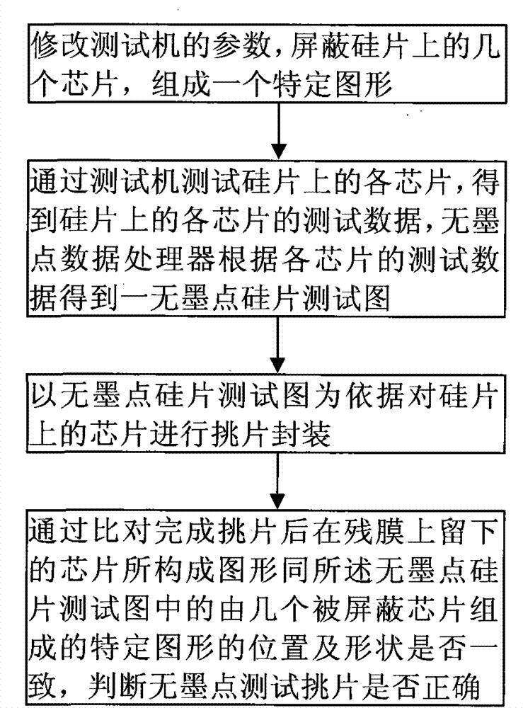
[0017] An embodiment of the alignment confirmation method of the ink-free dot test picking piece of the present invention is as follows: figure 1 shown, including the following steps:

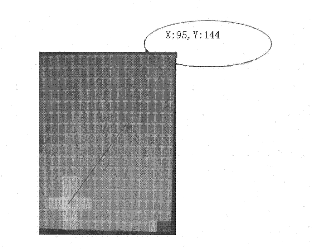
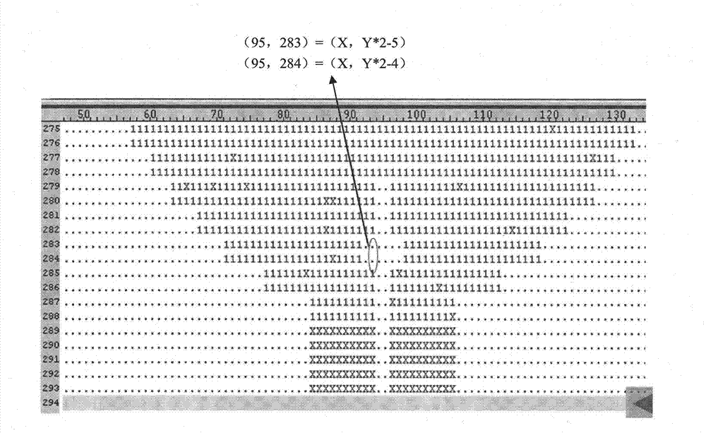
[0018] 1. Modify the parameters of the testing machine to mask several chips on the silicon wafer above the NOTCH (notch) of the silicon wafer to form a specific figure: a cross, such as figure 2 As shown, the coordinates of the two chips at the center of the cross are: X=95, Y=144. This specific graphic can be a cross, a rhombus, a triangle, an F, and the like.

[0019] Two. test each chip on the silicon wafer by a testing machine, obtain the test data of each chip on the silicon wafer, output to the data processor without ink dots, and the data processor without ink dots obtains a no ink dot data processor according to the test data of each chip Ink-dot silicon wafer test chart, the obtained no-ink-dot silicon wafer test chart will have the specific pattern composed of several shielded chi...


PUM


Abstract

The present invention discloses a chip picking and position aligning confirmation method for ink dot-free test, comprising the steps of: screening a plurality of chips on a wafer to form a specific pattern by modifying parameters of a test machine; testing all chips on the wafer through the test machine to obtain test data of all the chips on the wafer and enabling an ink dot-free data processor to obtain an ink dot-free wafer test chart according to the test data of all the chips; performing chip picking and packaging on the chips on the wafer according to the ink dot-free wafer test chart; and determining whether the chip picking for ink dot-free test is correct by comparing the position and shape of a pattern formed by the chips left on a residual film after chip picking with that of the specific pattern formed by the plurality of screened chips in the ink dot-free wafer test chart, to realize a correctness verification of chip picking on the wafer for the ink dot-free test. The chip picking and position aligning confirmation method for ink dot-free test can rapidly and correctly determine whether the chip picking for the ink dot-free test is correct, thereby easily realizing acorrectness verification of chip picking on a wafer for ink dot-free test, and has the advantages of simplicity and convenience.

Description

technical field [0001] The invention relates to a testing technology at the silicon wafer level, in particular to a method for confirming alignment of a chip in a test without ink dots. Background technique [0002] A general integrated circuit process can be divided into a wafer manufacturing stage, a die testing stage, and a chip packaging stage. After the silicon wafer with electrical characteristics is manufactured, the silicon wafer will be sent to the relevant testing machine for electrical testing of each chip on the silicon wafer, and the unqualified chips will be marked with ink to distinguish them. Whether the chip is qualified or not. Then, the tested silicon wafer will be sent to the packaging factory, so that the packaging factory can cut the silicon wafer into multiple chips, and pick out the qualified chips that have not been marked with ink dots and package them into packages. [0003] With the development of integrated circuit technology, the size of the c...

Claims


Application Information

Patent Timeline
Patent Type & Authority Patents(China)
IPC IPC(8): H01L21/66
Inventor 武建宏桑浚之郑东来
Owner SHANGHAI HUAHONG GRACE SEMICON MFG CORP
Why Eureka
Try Eureka