Manufacturing method of nail bed for PCB solder-mask printing

The technology of a PCB board and manufacturing method is applied in the field of PCB board solder mask printing, which can solve the problems of long time consumption, multiple nail bed boards 91, drilling time, and consumption, and achieve the advantages of easy management, saving board materials and drilling time Effect

Inactive Publication Date: 2012-07-04
SHENNAN CIRCUITS
View PDF0 Cites 1 Cited by
  • Summary
  • Abstract
  • Description
  • Claims
  • Application Information

AI Technical Summary

Problems solved by technology

[0010] The method for making the bed of nails in the above traditional method is relatively complicated, and it takes a long time to drill holes in the bed of nails board 91; Processing multiple different nails will consume more nail bed boards 91 and drilling time, and the management of nail beds is also more difficult

Method used


Image

  • Manufacturing method of nail bed for PCB solder-mask printing
  • Manufacturing method of nail bed for PCB solder-mask printing
  • Manufacturing method of nail bed for PCB solder-mask printing

Examples


Embodiment Construction

[0028] In order to make the object, technical solution and advantages of the present invention clearer, the present invention will be further described in detail below in conjunction with the accompanying drawings and embodiments. It should be understood that the specific embodiments described here are only used to explain the present invention, not to limit the present invention.

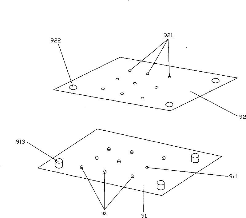
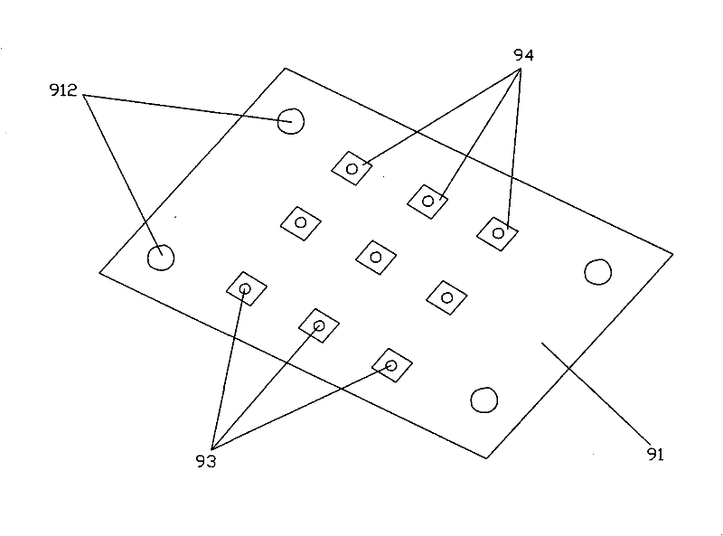
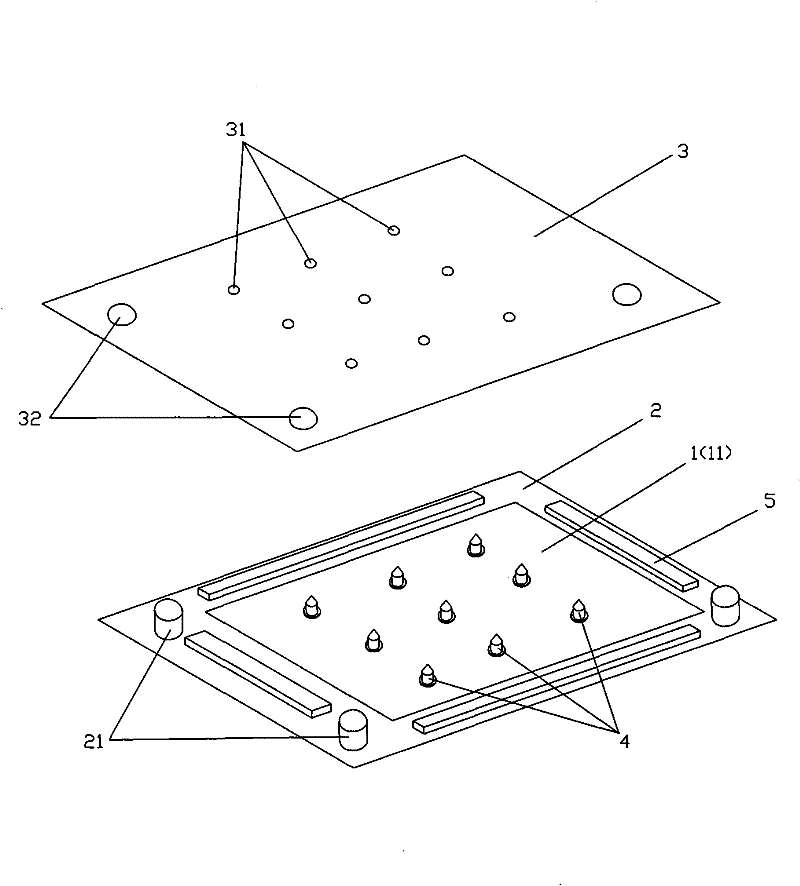
[0029] Such as image 3 and Figure 4 As shown, a method for manufacturing a PCB board solder resist printing nail bed provided by an embodiment of the present invention includes the following steps:

[0030] (1) A nail bed board 2 is set, and then double-sided adhesive tape 1 is pasted on this nail bed board 2; When the size of 1 is 18 "*24", the size of bed of nails 2 can be 20 "*26";

[0031] (2) Put the PCB board 3 flat on a horizontal surface (such as a desktop or the ground), put the needle 41 of the probe 4 into the fixing hole 31 on the PCB board 3, adjust the probe 4 to be perpendicular...


PUM


Abstract

The invention is suitable for the PCB (printed circuit board) solder-mask printing field and provides a manufacturing method of a nail bed for PCB solder-mask printing, wherein the method comprises the steps of: placing heads of probes on fixed orifices of the PCB; using a nail bed plate with double faced adhesive tapes to press the probes on the PCB plate to enable caps on the probes to adhere to the double faced adhesive tapes of the nail bed plate; and then overturning the PCB and the nail bed plate and adjusting the probes to be perpendicular to the PCB plate to finish the manufacturing of the nail bed. According to the manufacturing method of the invention, nail beds in different models needed by the solder-mask printing of the PCB are rapidly manufactured by using only one nail bed plate and changing the double faced adhesive tapes on the nail bed plate. Compared with the prior art, the method of the invention avoids drilling on the nail bed plate and saves a plurality of sheet materials and drilling time, besides, the nail bed is also convenient for management.

Description

technical field [0001] The invention belongs to the field of PCB board solder resist printing, and in particular relates to a method for manufacturing a PCB board solder resist printing nail bed. Background technique [0002] Such as figure 1 and figure 2 As shown, the manufacturing method of the traditional PCB board solder mask printing nail bed is as follows: [0003] (1) Material selection for the bed of nails 91: the material of the bed of nails 91 is generally copper-clad laminate; [0004] (2) Cutting of the nail bed board 91: the length and width of the nail bed board 91 are greater than the length and width of the PCB board 92 by more than 50.8 mm; [0005] (3) Nail bed plate 91 drilling: according to production needs, first drill the fixing hole 911 of φ0.8~φ1.5mm on the nail bed plate 91, the aperture of fixing hole 911 is a little smaller than the outer diameter of corresponding probe 93, with Make the interference fit between the fixing hole 911 and the pro...

Claims


Application Information

Patent Timeline
Patent Type & Authority Patents(China)
IPC IPC(8): H05K3/28
Inventor 张垚沙雷胡建红朱亮
Owner SHENNAN CIRCUITS
Why Eureka
Try Eureka