Testing and ageing adapter for semiconductor laser

An adapter and laser technology, used in semiconductor lasers, single semiconductor device testing, lasers, etc., can solve problems such as performance fluctuations of laser monomers, increase in return rates, and lower yields

Active Publication Date: 2011-07-20
WUXI LUMISOURCE TECH
View PDF5 Cites 18 Cited by
  • Summary
  • Abstract
  • Description
  • Claims
  • Application Information

AI Technical Summary

Problems solved by technology

[0003] However, due to the influence of many factors such as chip consistency and package consistency, the individual packaged laser monomers will have a certain degree of performance fluctuations, such as output power, wavelength, thermal resistance, etc.
These performance fluctuations will affect the overall performance of multi-chip integrated packaging, in other words, it may reduce yield, reduce service life and increase return rate

Method used


Image

  • Testing and ageing adapter for semiconductor laser
  • Testing and ageing adapter for semiconductor laser
  • Testing and ageing adapter for semiconductor laser

Examples


Embodiment Construction

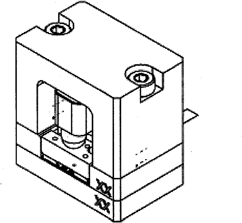
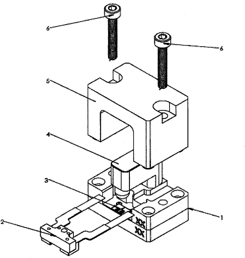
[0026] Such as Figure 1-9 As shown, a semiconductor laser test and burn-in adapter includes an adapter base 1, an adapter electrode 2, a semiconductor laser 3, a spring pressure head 4, an adapter cover 5, and cover fastening bolts 6. The semiconductor laser 3 is placed on the adapter base In the middle of 1, the semiconductor laser 3 is fixed and pressed by the adapter electrode 2 and the spring pressure head 4 above, and the adapter cover 5 provides mechanical protection for the adapter base 1, the adapter electrode 2, the semiconductor laser 3, and the spring pressure head 4. At the same time Provides a pressurized platform for diode laser testing and burn-in to ensure uniform cooling of adapter base 1.

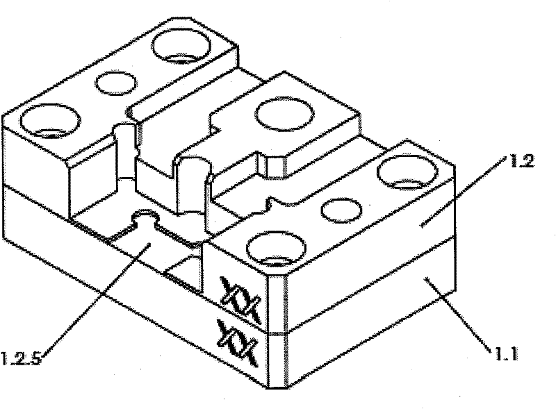
[0027] The adapter base 1 is composed of a lower half 1.1 and an upper half 1.2. After the lower half 1.1 and the upper half 1.2 are assembled, a rectangular opening 1.2.5 is formed for the semiconductor laser 3 to use. The lower half 1.1 is a cube, and a threaded hole 1...


PUM


Abstract

The invention discloses a testing and ageing adapter for a semiconductor laser, which comprises an adapter base, an adapter electrode, the semiconductor laser, a spring pressure head, an adapter upper cover and an upper cover fastening bolt, wherein the semiconductor laser is placed in the middle of the adapter base; the semiconductor laser is fixed and compacted by using the adapter electrode and the spring pressure head thereon; and the adapter upper cover provides a mechanical protection effect for the adapter base, the adapter electrode, the semiconductor laser and the spring pressure head, and simultaneously provides a compression platform for testing and ageing of the semiconductor laser to ensure uniform cooling of the adapter base. The invention discloses the testing and ageing screening adapter for the semiconductor laser Chip on Submount (CoS). The adapter provides a reliable and effective testing assessment tool for multiple required properties such as power consistency, wavelength consistency, thermal resistance consistency and the like when a plurality of chips are integrated and encapsulated. Based on the design, corresponding testing parameters are provided, and the feasibility of the design is verified.

Description

technical field [0001] The invention relates to a quality evaluation device of a semiconductor laser device Chip on Submount (CoS). Background technique [0002] High-power semiconductor lasers are often packaged in bar-chip, that is, multi-tube parallel packaging. Such packaging will inevitably result in high operating currents, which in turn will increase the requirements for the current-carrying capacity of the power supply circuit. Multi-tube series semiconductor laser chip packaging is a new type of semiconductor laser packaging technology that has emerged in recent years. There is no doubt that this technology is an effective way to greatly reduce the laser operating current. [0003] However, affected by many factors such as chip consistency and packaging consistency, the individually packaged laser monomers will have a certain degree of performance fluctuations, such as output power, wavelength, thermal resistance, and so on. These performance fluctuations will affe...

Claims


Application Information

Patent Timeline
Patent Type & Authority Applications(China)
IPC IPC(8): G01R31/26H01S5/00
Inventor 李大明潘华东张军
Owner WUXI LUMISOURCE TECH
Why Eureka
Try Eureka