Carrying tool for printed circuit board (PCB)

A technology for printed circuit boards and carriers, applied in the directions of printed circuits, printed circuit manufacturing, electrical components, etc., can solve the problems of low rigidity of printed circuit boards, poor electroplating effect of printed circuit boards, easy bending and deformation, etc., to achieve rapid electroplating. Effect

Inactive Publication Date: 2011-07-27
SHANGHAI MEADVILLE ELECTRONICS
View PDF4 Cites 3 Cited by
  • Summary
  • Abstract
  • Description
  • Claims
  • Application Information

AI Technical Summary

Problems solved by technology

However, when the thickness of the printed circuit board is less than 0.3mm, or even less than 0.1mm, due to the small rigidity of the printed circuit board, it is difficult to keep stable during the moving process, and it is easy to bend and deform. The plating effect of the printed circuit board after bending and deformation is poor, which cannot meet Requirements

Method used


Image

  • Carrying tool for printed circuit board (PCB)
  • Carrying tool for printed circuit board (PCB)
  • Carrying tool for printed circuit board (PCB)

Examples


Embodiment Construction

[0018] The present invention is described in detail below in conjunction with accompanying drawing:

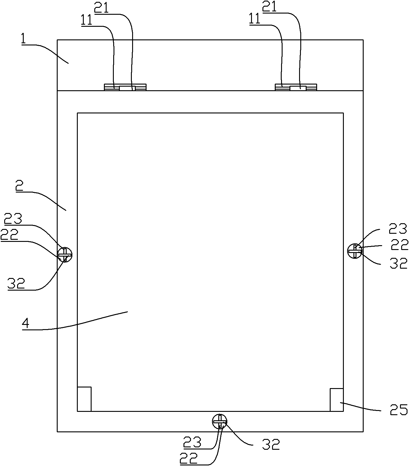
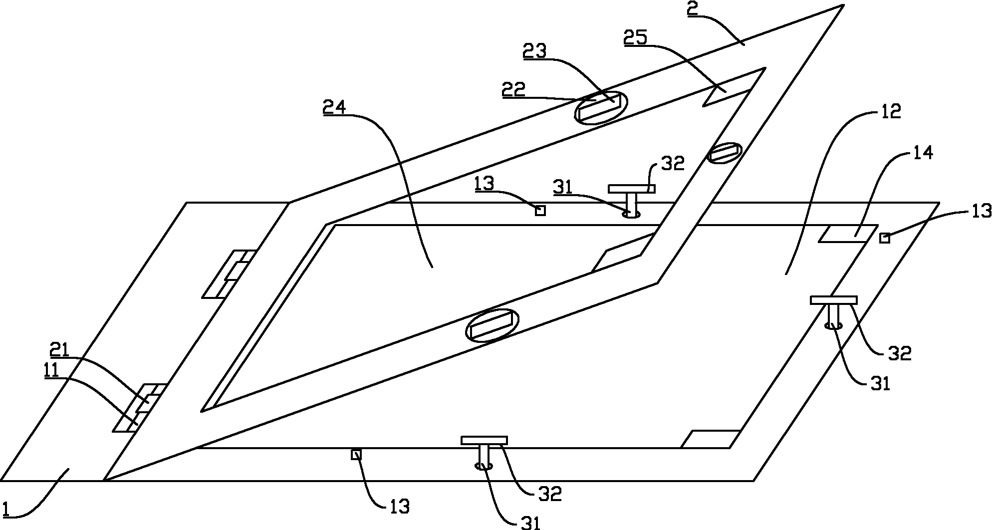
[0019] Such as figure 1 , figure 2 As shown, the printed circuit board carrier includes a first clamping frame 1 and a second clamping frame 2 . The first clamping frame 1 is provided with a first through hole 12 . The second clamping frame 2 is provided with a second through hole 24 .

[0020] Two shafts 11 are arranged on the first clamping frame 1 . Two sleeves 21 are arranged on the second clamping frame 2 , and the sleeves 21 are sleeved on the shaft 11 . The first clamping frame 1 is rotatably connected to the second clamping frame 2 , and when the first clamping frame 1 is fixed, the second clamping frame 2 can rotate around an axis 11 .

[0021] Three connecting rods 31 are rotatably installed on the first clamping frame 1 . Each connecting rod 31 passes through the first clamping frame 1 , one end of the connecting rod 31 is provided with an end cap (not shown ...


PUM


Abstract

The invention discloses a carrying tool for a printed circuit board (PCB), which is characterized by comprising a first clamping frame and a second clamping frame, wherein the first clamping frame is provided with a first through hole, and the second clamping frame is provided with a second through hole; the first clamping frame is connected with the second clamping frame in a relatively rotating way; and the carrying tool for the PCB also comprises a limit device which is used for limiting the PCB between the first clamping frame and the second clamping frame. The carrying tool for the PCB can be used for conveniently clamping the surrounding edge of the PCB, and ensures the PCB to stably move in the moving process without being bended and deformed. More particularly, the carrying tool guarantees the thinner PCB not to be bended and deformed, and realizes rapid electroplating for the thinner PCB.

Description

technical field [0001] The invention relates to a printed circuit board carrier. Background technique [0002] With the development of the electronics industry, the requirements for printed circuit boards are getting higher and higher. One of the requirements is that each printed circuit board is required to be thinner and thinner, so that more printed circuit boards can be installed to complete more complex functions when the total thickness of the circuit board remains unchanged. [0003] Electroplating is required in the production process of printed circuit boards, and one of the high-speed electroplating methods is vertical electroplating. The method adopted is to hang the printed circuit board on the carrier, the carrier drives the printed circuit board to pass through a plurality of electroplating tanks, and the printed circuit board is respectively immersed in the electroplating solution in the plurality of electroplating tanks for electroplating. [0004] When pro...

Claims


Application Information

Patent Timeline
IPC IPC(8): C25D17/06H05K3/18
Inventor 曹立志陶伟良黄伟
Owner SHANGHAI MEADVILLE ELECTRONICS
Why Eureka
Try Eureka