Plasma induced damage (PID) detection structure and manufacture method thereof

A damage detection and plasma technology, which is applied in semiconductor/solid-state device manufacturing, semiconductor/solid-state device testing/measurement, electric solid-state devices, etc., can solve the problem of inability to accurately detect the charge size of the antenna structure, etc.

Active Publication Date: 2011-08-03
SEMICON MFG INT (SHANGHAI) CORP
View PDF0 Cites 6 Cited by
  • Summary
  • Abstract
  • Description
  • Claims
  • Application Information

AI Technical Summary

Problems solved by technology

[0015] The invention provides a plasma damage detection structure to solve the problem that the existing plasma d

Method used


Image

  • Plasma induced damage (PID) detection structure and manufacture method thereof
  • Plasma induced damage (PID) detection structure and manufacture method thereof
  • Plasma induced damage (PID) detection structure and manufacture method thereof

Examples


no. 1 example

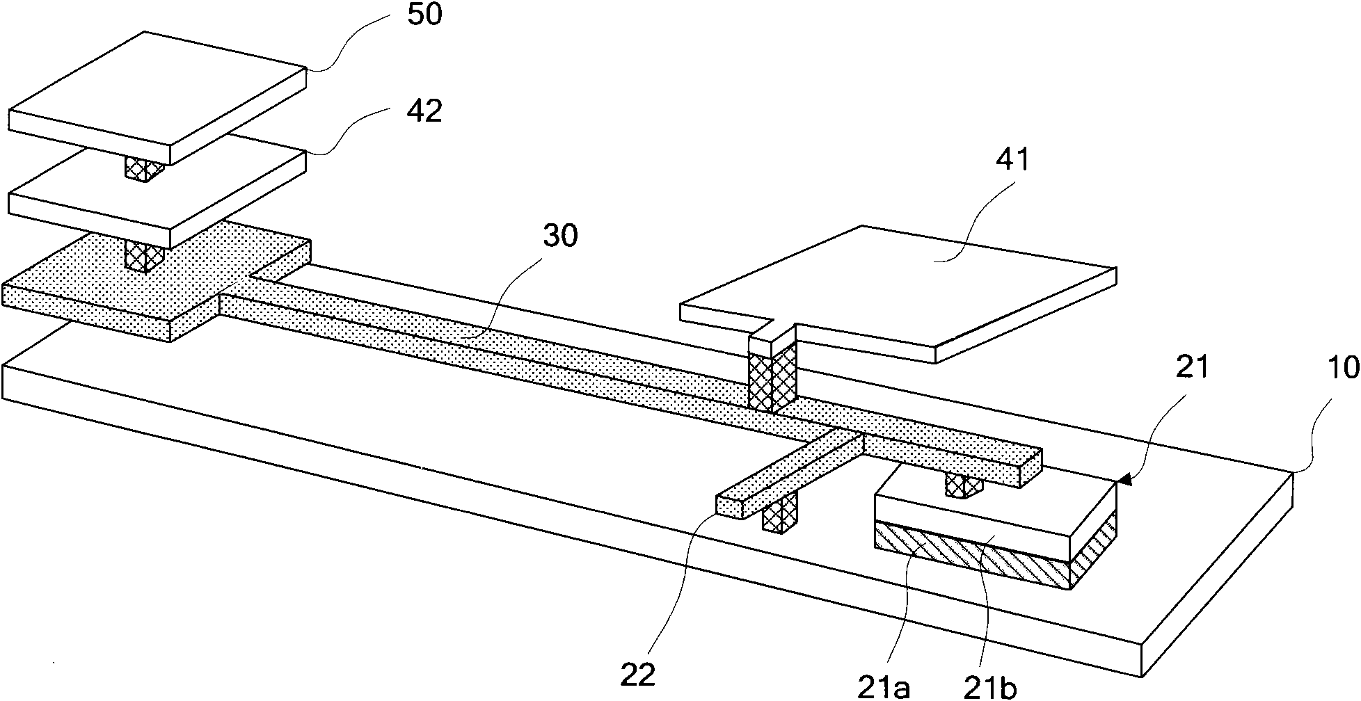
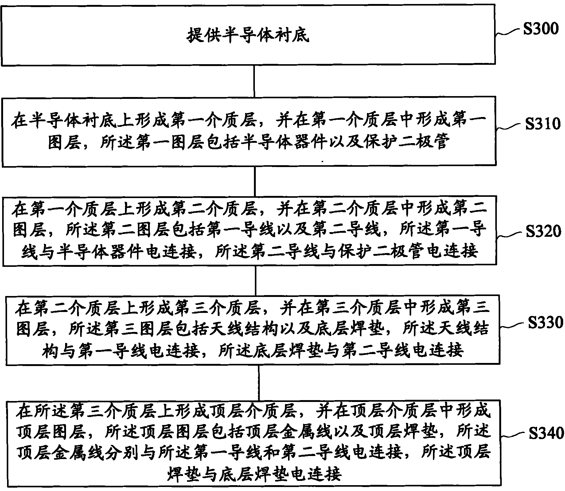
[0039] Please refer to figure 2 , which is a schematic diagram of the plasma damage detection structure provided by the first embodiment of the present invention, such as figure 2 As shown, the plasma damage detection structure provided by the first embodiment of the present invention includes: a semiconductor substrate 100 , a first layer, a second layer, a third layer and a top layer.

[0040] The first layer is disposed in a first dielectric layer, and the first layer includes a semiconductor device 210 and a protection diode 220 formed on the semiconductor substrate 100;

[0041] The second layer is arranged in the second dielectric layer, the second layer includes a first wire 310 and a second wire 320, the first wire 310 is electrically connected to the semiconductor device 210, and the second wire 320 electrically connected with the protection diode 220;

[0042] The third layer is disposed in the third dielectric layer, the third layer includes an antenna structure...

no. 2 example

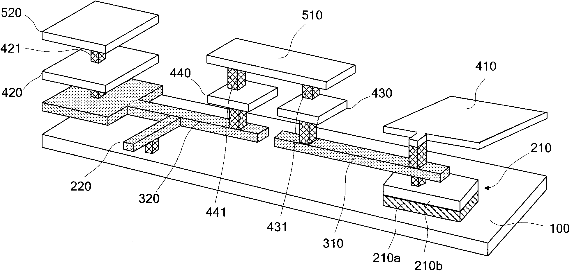
[0064] Please refer to Figure 5 , which is a schematic diagram of the plasma damage detection structure provided by the second embodiment of the present invention. The difference from the first embodiment of the present invention is that the plasma damage detection structure provided by the second embodiment of the present invention also includes covering the third The intermediate medium layer of the medium layer and a plurality of intermediate layers arranged in the intermediate medium layer.

[0065]Specifically, wherein each intermediate layer comprises an intermediate layer welding pad 620, a first intermediate layer metal line 630 and a second intermediate layer metal line 640, and the intermediate layer welding pad 620 is connected to the bottom layer welding pad 420 and the top layer welding pad respectively. 520, the first middle layer metal line 630 is electrically connected to the first bottom layer metal line 430 and the top layer metal line 510, and the second mi...


PUM


Abstract

The invention discloses a plasma induced damage (PID) detection structure and a manufacture method thereof. The PID structure comprises a semiconductor substrate, a first coverage, a second coverage, a third coverage and a top coverage, wherein the first coverage is arranged in a first medium layer and comprises a semiconductor device and a protection diode formed on the semiconductor substrate; the second coverage is arranged in a second medium layer and comprises a first wire and a second wire, wherein the first wire is electrically connected with the semiconductor device, and the second wire is electrically connected with the protection diode; the third coverage is arranged in a third medium layer and comprises an antenna structure and a bottom welding pad, wherein the antenna structure is electrically connected with the first wire, and the bottom welding pad is electrically connected with the second wire; the top coverage is arranged in a top medium layer and comprises a top metalline and a top welding pad, wherein the top metal line is electrically connected with the first wire and the second wire; and the top welding pad is electrically connected with the bottom welding pad. According to the PID detection structure and the manufacture method thereof, the strength of antenna effect can be accurately detected.

Description

technical field [0001] The invention relates to the field of integrated circuit manufacturing, in particular to a plasma damage detection structure and a manufacturing method thereof. Background technique [0002] In the manufacturing process of semiconductor devices, many process steps such as dry etching, ion implantation, and chemical vapor deposition use plasma. In theory, the plasma is electrically neutral to the outside, that is, positive and negative ions The numbers are equal. But in fact, the positive ions and negative ions entering the local area of ​​the wafer are not equal, which leads to the generation of a large number of free charges, making the conductors such as metal wires or polysilicon exposed to the plasma environment like antennas. Collect these free charges. The longer and larger these antennas are, the more charge they can collect. When the charge collected by these antennas reaches a certain level, a discharge phenomenon will occur. The above disc...

Claims


Application Information

Patent Timeline
IPC IPC(8): H01L23/544H01L21/71H01L21/66
Inventor 马瑾怡郑雅文王晓韬许晓锋
Owner SEMICON MFG INT (SHANGHAI) CORP
Why Eureka
Try Eureka