Focal plane assembly capable of realizing same viewing field splicing

A field of view splicing and focal plane technology, which is applied in the field of aerospace optical remote sensors, can solve the problems of difficulty in seamless splicing of the same field of view, inability to achieve seamless splicing, and reduced electrical performance, so as to improve the level of integration and functional density. , to avoid mutual interference, to expand the effect of the coverage width

Inactive Publication Date: 2011-08-03
BEIJING RES INST OF SPATIAL MECHANICAL & ELECTRICAL TECH
View PDF5 Cites 6 Cited by
  • Summary
  • Abstract
  • Description
  • Claims
  • Application Information

AI Technical Summary

Problems solved by technology

It is generally believed that the prerequisite for seamless splicing of the same field of view is that the physical packaging size of the photosensitive device in the splicing direction is at least twice the length of the photosensitive surface of the photosensitive device in the splicing direction; It is difficult to achieve seamless splicing in the same field of view when the photosensitive surface of the photosensitive device whose package size is greater than 2 times the length in the splicing direction
Due to the influence of the peripheral circuit and package of the photosensitive device, the package size of the device is often large, especially for highly integrated photosensitive devices such as CMOS. Due to the integration of many signal processing circuits and multiple functions, the package size is easily larger than twice that of the photosensitive device. The length of the surface makes it impossible to achieve seamless splicing with traditional methods
If the method of artificially reducing the package size is used, such as cutting the pins short, the electrical performance may be reduced, especially in the case of high circuit frequency
At the same time, it will also bring difficulties to the electrical equipment.

Method used


Image

  • Focal plane assembly capable of realizing same viewing field splicing
  • Focal plane assembly capable of realizing same viewing field splicing
  • Focal plane assembly capable of realizing same viewing field splicing

Examples


Embodiment Construction

[0020] Specific embodiments of the present invention will be further described in detail below in conjunction with the accompanying drawings.

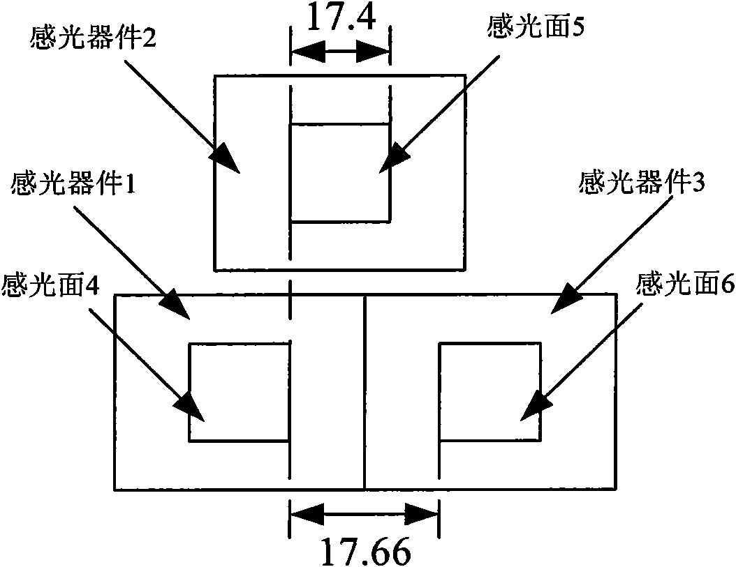
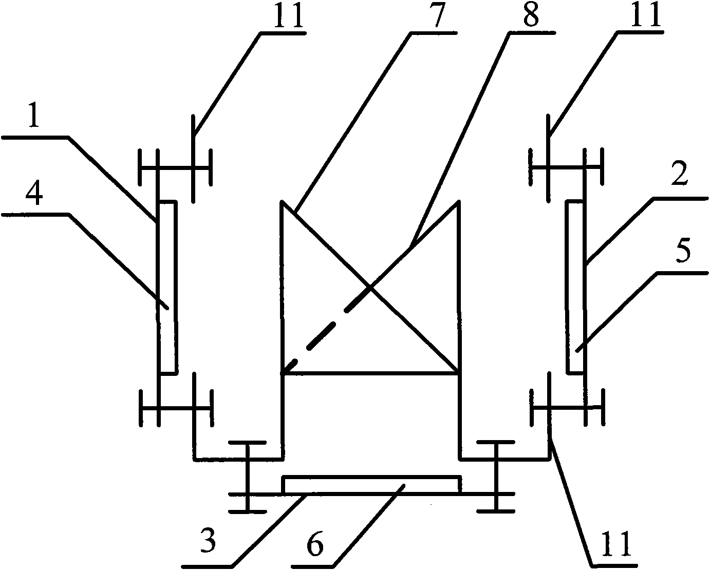
[0021] Such as figure 1 As shown, the present invention aims at the problem of missing pixels when the physical packaging size of the photosensitive device in the splicing direction is greater than twice the length of the photosensitive surface of the photosensitive device in the splicing direction. A photosensitive device refers to a photoelectric conversion device, which can be a linear array, an area array, etc., including a photosensitive surface and its peripheral packaging, such as a common CMOS photosensitive device or a CCD photosensitive device. The photosensitive surface of the photosensitive device is a square or rectangular photosensitive area composed of independent square or rectangular photosensitive pixels, and its center is generally located at the center of the photosensitive device. The length of the border between ...


PUM


Abstract

The invention discloses a focal plane assembly capable of realizing same viewing field splicing, belonging to the technical field of aerospace optical remote sensors. The focal plane assembly comprises three imaging circuit boards, three photosensitive devices, two reflecting mirrors, two bosses and a structural frame, wherein the three photosensitive devices are respectively positioned on three imaging circuit boards and are distributed on three planes; reflecting mirrors are cross to realize twice reflection and once perpendicular incidence, thereby overcoming the detect that image elementsare leaked when a big-shell photosensitive device is spliced by the traditional two-surface layout; and the physical structures of the photosensitive devices or the circuit board can be prevented from mutually interfering on the splicing direction, the photosensitive surfaces of the three photosensitive devices are connected end to end, and parts of regions of the junction are overlapped so as torealize seamless splicing. According to the focal plane assembly, three (which can be expanded to multiple pieces) photosensitive devices, especially three big-shell devices, can be subjected to seamless same viewing field splicing, the size requirement on an imaging circuit is lowered, the performance is improved, the cost is lowered, and the focal plane size is enlarged so as to enlarge the ground coverage width.

Description

technical field [0001] The invention relates to a splicing focal plane assembly with the same field of view, which belongs to the technical field of aerospace optical remote sensors. Background technique [0002] With the rapid development of aerospace optical remote sensor technology, the requirements for the large field of view of optical remote sensors are getting higher and higher. At present, the length of the focal plane has reached the order of several hundred millimeters. Large, often using the splicing method. At present, the photosensitive device and the circuit board on the focal plane assembly based on the reflective surface are arranged on two planes. It is generally believed that the prerequisite for seamless splicing of the same field of view is that the physical package size of the photosensitive device in the splicing direction is at least twice the length of the photosensitive surface of the photosensitive device in the splicing direction; the physical pac...

Claims


Application Information

Patent Timeline
Patent Type & Authority Applications(China)
IPC IPC(8): H01L25/065H01L31/0232H01L27/146G02B7/182G02B17/06
Inventor 姜伟高卫军黄巧林郭悦齐文雯王军赵野蔺宇辉
Owner BEIJING RES INST OF SPATIAL MECHANICAL & ELECTRICAL TECH
Why Eureka
Try Eureka