Magnetic field sensor

A sensor and sensor device technology, which can be used in the measurement of geometric arrangement of magnetic sensing elements, instruments, nano-magnetics, etc., and can solve problems such as damage to AMR elements.

Active Publication Date: 2011-08-10
NXP BV
View PDF10 Cites 14 Cited by
  • Summary
  • Abstract
  • Description
  • Claims
  • Application Information

AI Technical Summary

Problems solved by technology

The required handling may damage the AMR element in

Method used


Image

  • Magnetic field sensor
  • Magnetic field sensor
  • Magnetic field sensor

Examples


Embodiment Construction

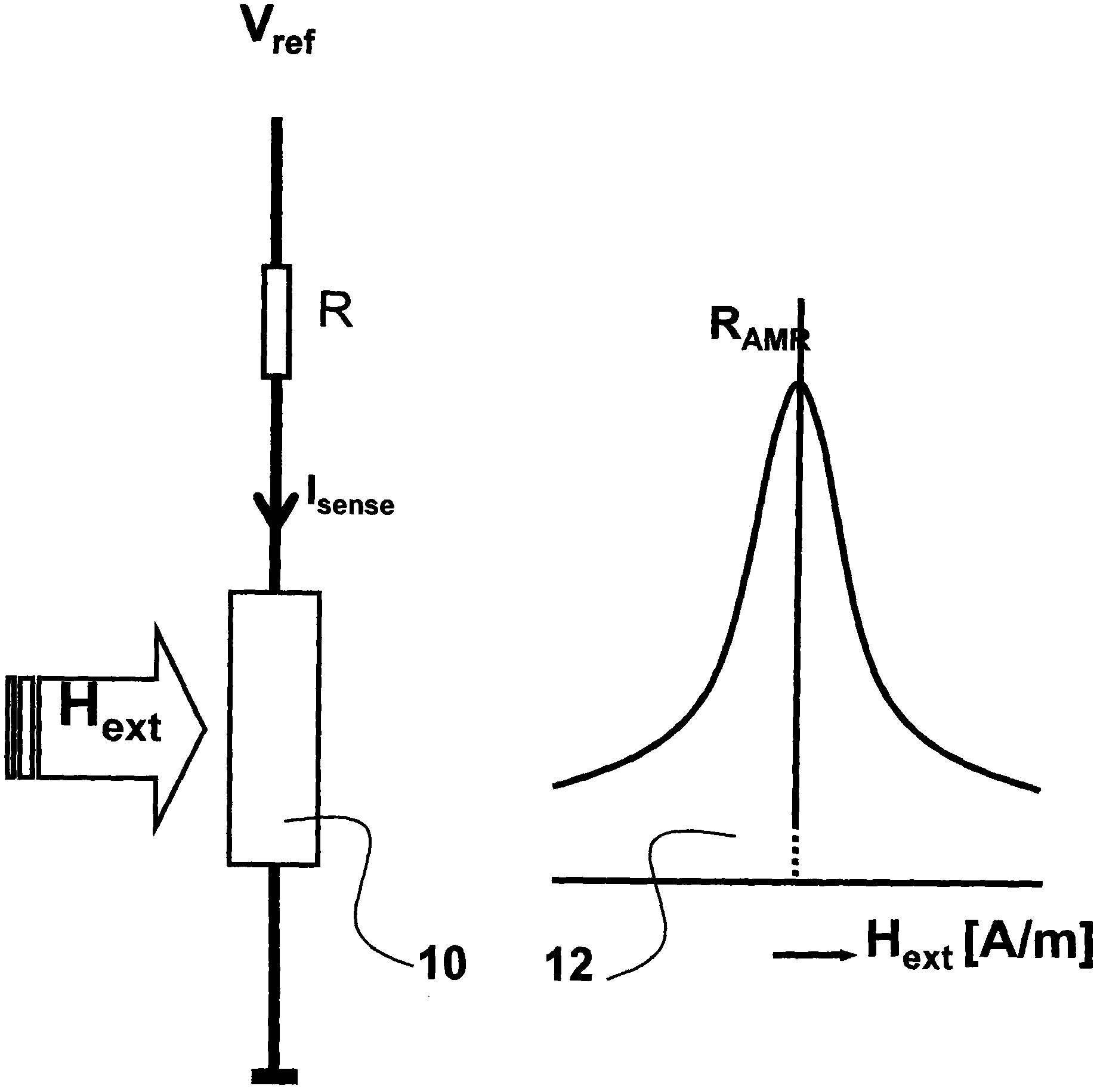
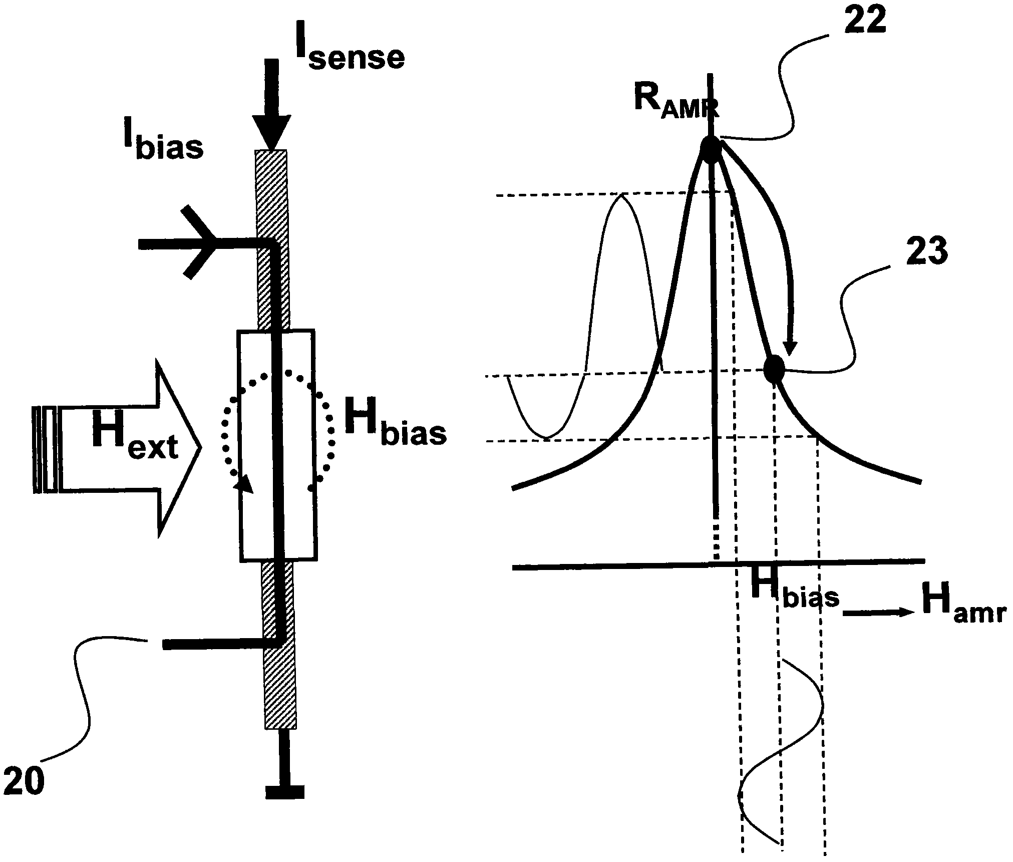
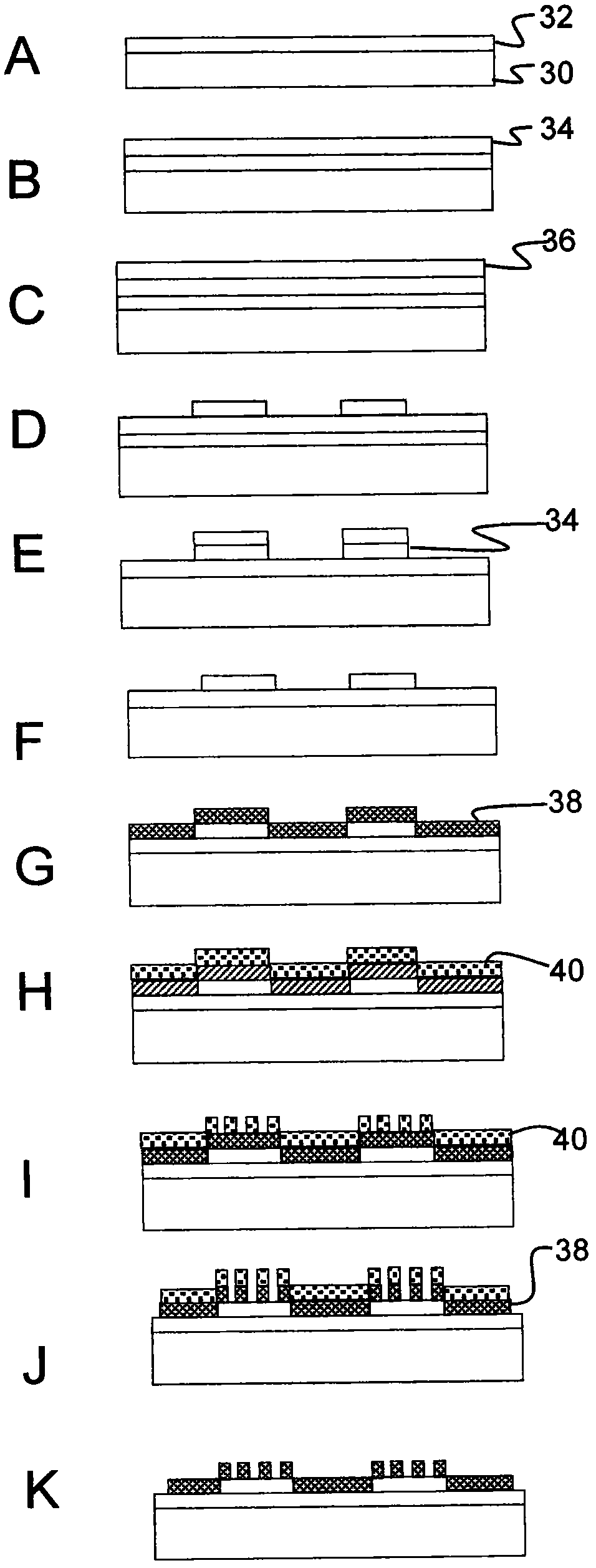
[0042] The present invention proposes a magnetoresistive sensor device integrated with an IC. The sensor is used to sense the strength and / or direction of an external magnetic field. For example, such an external magnetic field may be rotated for the object for which the angular orientation is to be sensed.

[0043] A metal layer of an IC structure (eg, CMOS) is patterned to define at least first and second contact regions. Metal connecting plugs are arranged below the first and second contact areas of the metal layer for making contact with terminals of the integrated circuit. A layer of magnetoresistive material overlies the metal layer and is separated by a dielectric layer. The second metal connection plug extends upward from the metal layer to the magnetoresistive material layer (sensor layer). Thus, a sensor layer is formed on top of the layers of the IC structure. The invention is generally applicable to magnetoresistive sensors, but is of particular interest for an...


PUM

PropertyMeasurementUnit
Diameteraaaaaaaaaa

Abstract

An MR sensor arrangement is integrated with an IC. A metal layer of the IC structure (e.g. CMOS) is patterned to define at least first and second contact regions. Metal connecting plugs are provided below the first and second contact regions of the metal layer for making contact to terminals of the integrated circuit. A magnetoresistive material layer is above the metal layer and separated by a dielectric layer. Second metal connecting plugs extend up from the metal layer to an MR sensor layer. The sensor layer is thus formed over the top of the layers of the IC structure.

Description

technical field [0001] The present invention relates to a magnetic sensor and a magnetic sensor. In particular, the invention relates to an MR (magnetoresistive) sensor, such as an anisotropic magnetoresistive (AMR) sensor. Background technique [0002] Magnetic sensors are becoming increasingly important in various industries. Specifically in the automotive industry, the modern traffic field has seen the presence of various sensors such as parking sensors, angle sensors, ABS (automatic braking system) sensors and tire pressure sensors for improving comfort and safety. Magnetic sensors are especially important in automotive applications because magnetic fields readily penetrate most materials. Unlike eg optical sensors, magnetic sensors are very insensitive to dirt. [0003] Several different magnetic sensor technologies are currently available, such as sensors based on the Hall effect or the magnetoresistive effect. Anisotropic magnetoresistive (AMR) and giant magnetore...

Claims


Application Information

Patent Timeline
IPC IPC(8): G01R33/09
CPCG01R33/0052B82Y25/00G01R33/096G01R33/093G01R33/0005
Inventor 弗德里克·威廉·毛里提斯·范赫蒙特马克·艾斯勒安德烈亚斯·伯纳德斯·玛丽亚·扬斯曼罗伯特斯·亚德里恩斯·玛丽亚·沃特斯
Owner NXP BV
Why Eureka
Try Eureka