Substrate holding member, substrate processing apparatus, and substrate processing method

A substrate holding and substrate technology, applied in electrical components, semiconductor/solid-state device manufacturing, ion implantation and plating, etc., can solve the problems of chip outer edge damage, short circuit, chip breakage, etc.

Active Publication Date: 2011-08-10
SHIBAURA MECHATRONICS CORP
View PDF1 Cites 8 Cited by
  • Summary
  • Abstract
  • Description
  • Claims
  • Application Information

AI Technical Summary

Problems solved by technology

[0004] Especially when the substrate to be processed is a very thin semiconductor wafer, the outer edge of the wafer is likely to be damaged due to the contact between the outer edge of the wafer and the holder, etc.
The problem here is that if fragments of the wafer fall on the handling hand or the electrostatic chuck, the following problems are worrying: the fragments are caught between them and the wafer, causing damage to the element forming surface of the wafer; causing the wafer to break; if The surface of the electrostatic chuck is made of soft materials such as polyimide, and debris will enter and reach the electrodes for the electrostatic chuck, causing short circuits, etc.

Method used


Image

  • Substrate holding member, substrate processing apparatus, and substrate processing method
  • Substrate holding member, substrate processing apparatus, and substrate processing method
  • Substrate holding member, substrate processing apparatus, and substrate processing method

Examples


Embodiment Construction

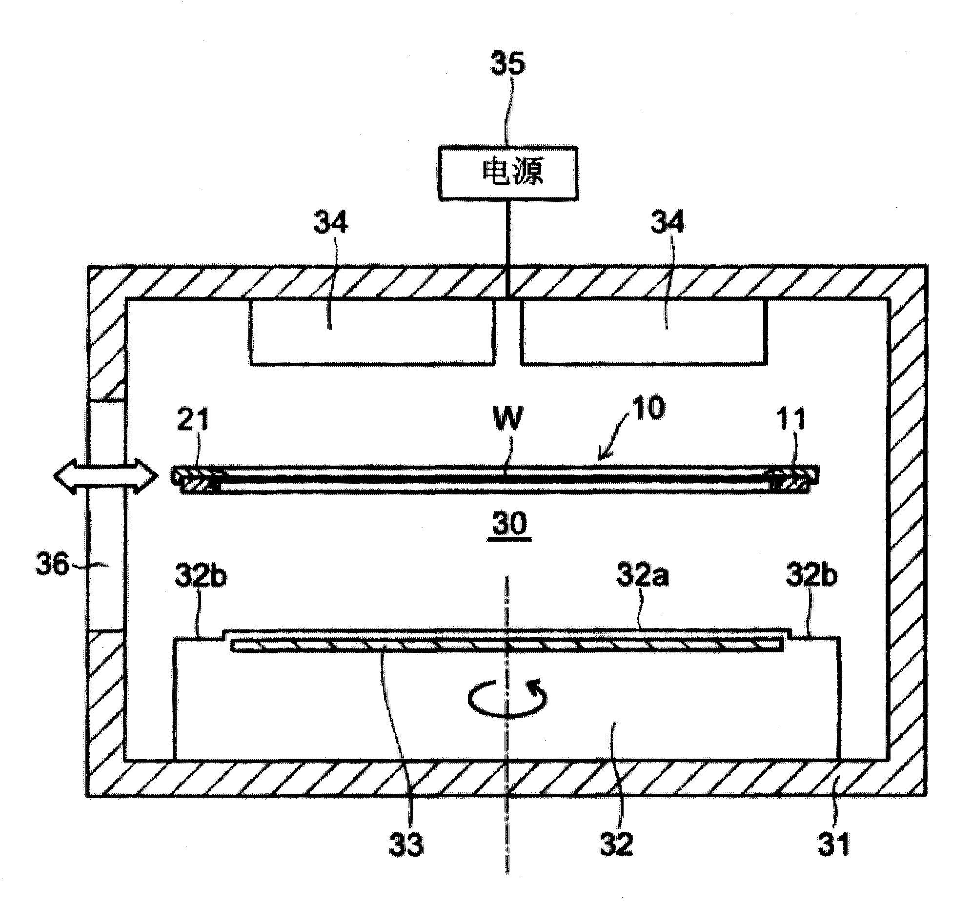
[0017] Hereinafter, embodiments of the present invention will be described with reference to the drawings. In the embodiment of the present invention, a specific example in which, for example, a semiconductor wafer is used as a substrate to be processed and sputtering film formation is performed on the semiconductor wafer will be described.

[0018] In the embodiment, the semiconductor wafer to be processed is very thin, for example, has a thickness of 10 to 100 μm, more specifically, about 50 μm. In the present embodiment, the thin semiconductor wafer is carried into and out of the processing chamber while being held by the holding member.

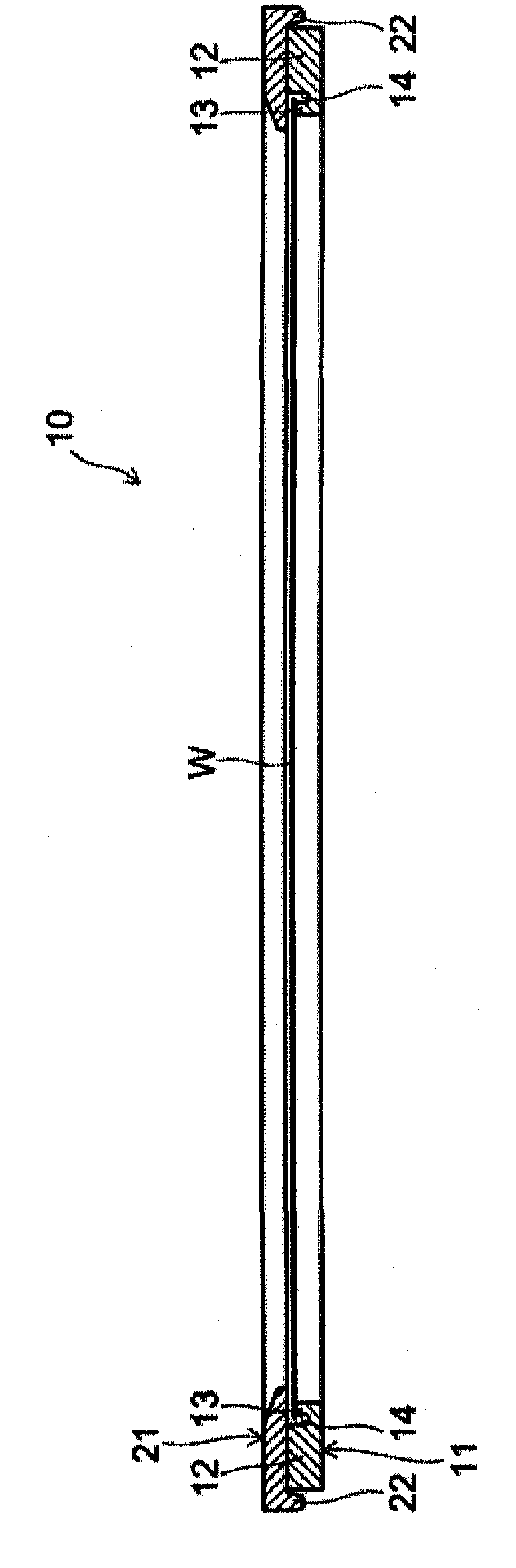
[0019] figure 1 A schematic cross-sectional view of the holding member 10 is shown. Moreover, in figure 1 2 also shows the semiconductor wafer W held by the holding member 10 at the same time.

[0020] The holding member 10 is composed of an annular holder 11 and a similarly annular mask 21 . The above-mentioned holder 11 and mask 21...


PUM

PropertyMeasurementUnit
diameteraaaaaaaaaa

Abstract

A substrate processing apparatus includes a ring-shaped tray including a substrate support configured to support an outer edge portion of a substrate, a mask support provided on an outer periphery side of the substrate support and projected above an upper surface of the substrate support, and a recess provided between the substrate support and the mask support; a ring-shaped mask covering the recess and the substrate support of the tray in a state where the mask is superposed on the mask support of the tray; and a rotary stage including an electrostatic adsorption surface and a tray mounting portion provided on an outer periphery side of the electrostatic adsorption surface and below the electrostatic adsorption surface. The outer edge portion of the substrate is projected toward the tray mounting portion side from the electrostatic adsorption surface. The substrate support is spaced below the outer edge portion of the substrate. The mask is spaced above the outer edge portion of the substrate.

Description

technical field [0001] The invention relates to a substrate holding member, a substrate processing device, and a substrate processing method, and is especially applied to the processing of a thin substrate. Background technique [0002] In substrate processing in which thin film formation, surface modification, dry etching, and the like are performed on a substrate in vacuum, there are cases where the substrate is processed on a holder. For example, Patent Document 1 discloses that a ring chuck is placed on a substrate placed in a concave portion of a bottomed holder, and in this state, the holder is electrostatically attracted to the electrostatic chuck to process the substrate. . [0003] Patent Document 1: Japanese Patent Laid-Open No. 2003-59998 [0004] In particular, when the substrate to be processed is a very thin semiconductor wafer, damage to the outer edge of the wafer is likely to occur due to, for example, contact between the outer edge of the wafer and the ho...

Claims


Application Information

Patent Timeline
Patent Type & Authority Applications(China)
IPC IPC(8): H01L21/683C23C14/34H01L21/205H01L21/3065
CPCH01L21/68735C23C14/042H01L21/68721C23C14/50C23C14/34H01L21/205H01L21/3065H01L21/683
Inventor 小暮公男
Owner SHIBAURA MECHATRONICS CORP
Why Eureka
Try Eureka