Array substrate, liquid crystal panel and liquid crystal displayer

An array substrate and base substrate technology, applied in the field of liquid crystal display, can solve problems such as lowering LCD display quality, poor LCD display, irregular slit patterns, etc., and achieves the goal of improving display quality, not affecting aperture ratio, and avoiding dark spots Effect

Active Publication Date: 2011-08-17
BOE TECH GRP CO LTD +1
View PDF6 Cites 26 Cited by
  • Summary
  • Abstract
  • Description
  • Claims
  • Application Information

AI Technical Summary

Problems solved by technology

[0004] In the research process of realizing the present invention, the inventors found that the array substrate with the above structure has the following defects when displaying images: since the center line of the pixel unit is the intersection of the inclined slits on both sides, it is not a regular slit pattern, such as figure 2 shown
[0005] Therefore, the LCD with the above structure has poor display, which reduces the display quality of the LCD.

Method used


Image

  • Array substrate, liquid crystal panel and liquid crystal displayer
  • Array substrate, liquid crystal panel and liquid crystal displayer
  • Array substrate, liquid crystal panel and liquid crystal displayer

Examples


Embodiment 1

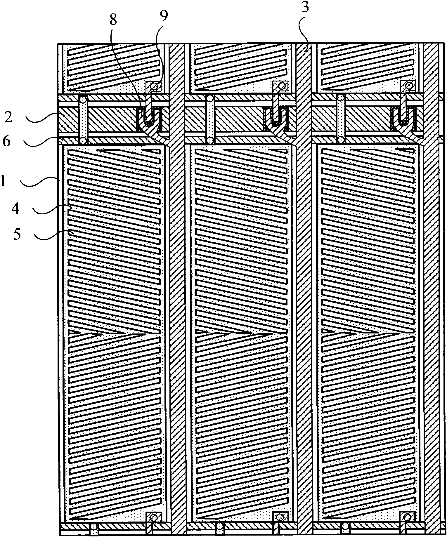
[0032] Figure 4A A partial top view structural schematic diagram of an array substrate provided in Embodiment 1 of the present invention (the top view herein does not show an insulating layer), the array substrate includes a first base substrate 1, and a gate arranged on the first base substrate 1 Lines 2 and data lines 3, a plurality of gate lines 2 and data lines 3 that intersect horizontally and vertically surround a plurality of pixel units arranged in a matrix, and each pixel unit includes a first electrode 4 and a second electrode 5 with slits and TFT switches, the first electrode 4 and the second electrode 5 are used to form an electric field for driving liquid crystal molecules. The array substrate usually also includes a common electrode line 6 for communicating with the second electrode 5 . In each pixel unit, the first electrode 4 with a slit includes a first region 41 and a second region 42; the gate line 2 and the TFT switch are arranged in the pattern of the fi...

Embodiment 2

[0039] Figure 5 The partial top view structural diagram of the array substrate provided by Embodiment 2 of the present invention is different from Embodiment 1 in that the first electrode 4 is not limited to include two independent regions, but may also include four independent regions. The four areas are denoted as the first area 41 , the second area 42 , the third area 43 and the fourth area 44 , and the gate line 2 is respectively connected to each area of ​​the first electrode 4 through the drain electrode 9 of the TFT switch. The specific connection form can be as follows Figure 5 As shown, the drain electrode 9 is connected by designing the pattern of four branches, and two or four TFT switches may be provided so that the drain electrode 9 is respectively connected to each region. The number of TFT switches can be set in consideration of factors such as the aperture ratio of the pixel unit, the driving current required by each area of ​​the first electrode 4 , and the...

Embodiment 3

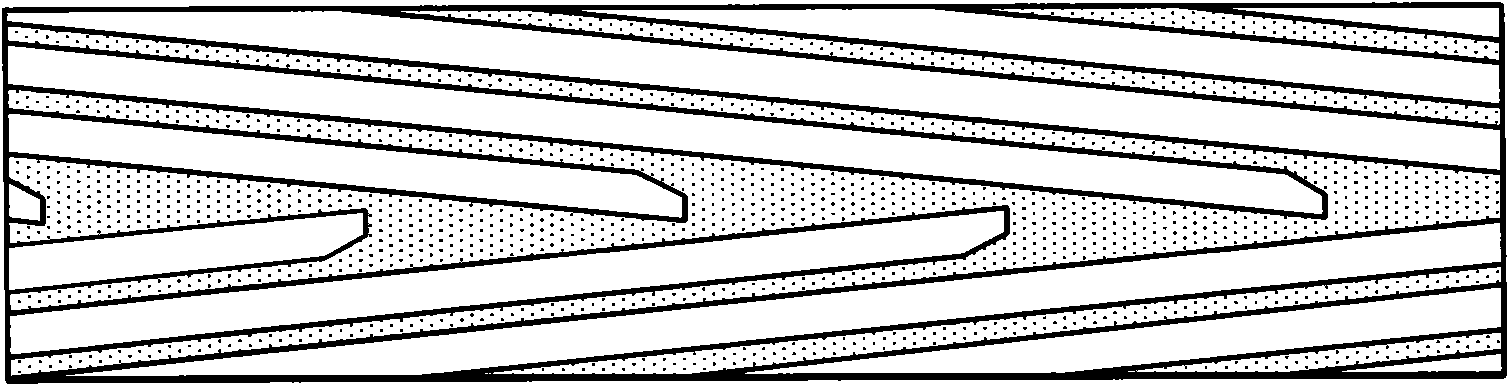
[0044] Figure 6A The top-view structural diagram of the array substrate provided in Embodiment 3 of the present invention, this embodiment can be based on the foregoing embodiments, and the sides of the first region 41 and the second region 42 of the first electrode 4 adjacent to the gate line 2 are sloped sides, the sloped sides are respectively parallel to the slits of their respective regions, such as Figure 6B shown as Figure 6A Schematic diagram of the zoomed-in structure inside the middle circle.

[0045] In order to match the shape of the first electrode 4 of the pixel unit, the shape of the gate line 2 located between the first region 41 and the second region 42 is preferably triangular, and the shape of the triangle matches the inclined side, that is, the edge of the triangle is roughly parallel to the inclined side . Therefore, the gap between the first electrode 4 and the gate line 2 is reduced as much as possible, and the aperture ratio of the pixel unit is i...


PUM

PropertyMeasurementUnit
angleaaaaaaaaaa

Abstract

The invention discloses an array substrate, a liquid crystal panel and a liquid crystal displayer, wherein the array substrate comprises a first lining substrate, and grating lines and data wires that form a plurality of pixel units in a surrounding way; each pixel unit comprises a first electrode with a narrow seam, a second electrode and a thin-film transistor switch; the first electrode and the second electrode are used for forming electric field that can drive the liquid crystal molecules, wherein the first electrode comprises more than two independent regions; the grating lines and the thin-film transistor switch are arranged among the patterns in all regions of the first electrode; the thin-film transistor switch comprises a grid electrode, a source electrode and a drain electrode; the grid electrode is connected with the grating lines; the source electrode is connected with the data wires; and the drain electrode is connected with all regions respectively. In the invention, theregions of the first electrode with different inclination direction of narrow seams can be divided by the grating lines and the thin-film transistor switch, so that the liquid crystal molecule regions with disorganized deflection can be blocked by the black matrix and the displaying quality of wide visual angle can be improved.

Description

technical field [0001] The invention relates to liquid crystal display technology, in particular to an array substrate, a liquid crystal panel and a liquid crystal display. Background technique [0002] A liquid crystal display is a commonly used flat panel display at present, and a thin film transistor liquid crystal display (ThinFilm Transistor Liquid Crystal Display, TFT-LCD for short) is a mainstream product in the liquid crystal display. According to different driving methods, LCD can be divided into Twisted Nematic (TN for short), In-Plane Switching (IPS for short), Fringe Field Switching (FFS for short) and advanced Advanced-Super Dimensional Switching (Advanced-Super Dimensional Switching; AD-SDS for short), for IPS, FFS and AD-SDS LCDs, the first electrode and the second electrode used to form the driving electric field are commonly called The pixel electrodes and the common electrodes are all formed on the array substrate. The difference is that the first electro...

Claims


Application Information

Patent Timeline
Patent Type & Authority Applications(China)
IPC IPC(8): G02F1/1362G02F1/1343G02F1/1368H01L27/12
CPCH01L29/41733G02F1/134363H01L27/12G02F1/133512G02F2001/134372G02F1/136286G02F1/134372H01L27/124G02F1/1368
Inventor 宋勇志薛建设郝昭慧林成武
Owner BOE TECH GRP CO LTD
Why Eureka
Try Eureka